Semiconductor device and a method of manufacturing the same

a technology of semiconductor devices and semiconductors, applied in the direction of semiconductor devices, basic electric elements, electrical appliances, etc., can solve the problems of increasing power consumption, rom data destruction, and undissolved problems, and achieve the effect of improving the reliability of field effect transistors

Inactive Publication Date: 2006-06-15
RENESAS TECH CORP
View PDF2 Cites 224 Cited by
  • Summary
  • Abstract
  • Description
  • Claims
  • Application Information

AI Technical Summary

Benefits of technology

[0015] In a semiconductor device having an element isolation region, reliability of a field effect transistor can be improved by reducing the inconvenience, that is, flow of a leak current resulting from crystal defects, for example, an undesired leak current between the source and drain of the field effect transistor.

Problems solved by technology

A variety of studies have been made to achieve this, but several problems have still remained undissolved.
It has however become apparent that when the width of the element isolation region is set to less than 0.3 μm, an undesired leak current occurs between the source and drain of field effect transistors constituting the mask ROM and causes problems such as an increase in power consumption or destruction of ROM data.
It is presumed that as a result, the stress triggers formation of crystal defects in the active region and causes the above-described leak current.

Method used


Image

  • Semiconductor device and a method of manufacturing the same
  • Semiconductor device and a method of manufacturing the same
  • Semiconductor device and a method of manufacturing the same

Examples


embodiment 1

[0059]FIG. 39 is a chip block diagram showing a main circuit block inside of a semiconductor chip of a semiconductor device having, mounted thereover, a flash memory according to Embodiment 1.

[0060] A semiconductor device FM includes a memory array MA of a flash memory disposed over more than half of the main surface of a semiconductor substrate, a decoder SD for selecting a memory cell, a sense amplifier data latch SL for amplifying a feeble signal and storing data, and a logic portion for controlling this circuit portion. It further includes a mask ROM region MR and a power source DC. The memory array MA has a predetermined number of word lines WL disposed at a predetermined pitch, a predetermined number of bit lines disposed at a predetermined pitch in a direction vertical to the word lines, and many memory cells arranged in a lattice shape at substantial intersections between the word lines and the bit lines.

[0061] One example of manufacturing methods of the flash memory accor...

embodiment 2

[0100] A manufacturing method of a flash memory according to Embodiment 2 will hereinafter be described in the order of steps based on FIGS. 15 to 29. Here, one application example of the present invention to a manufacturing method of an AND type flash memory having an assist gate (AG) will be described.

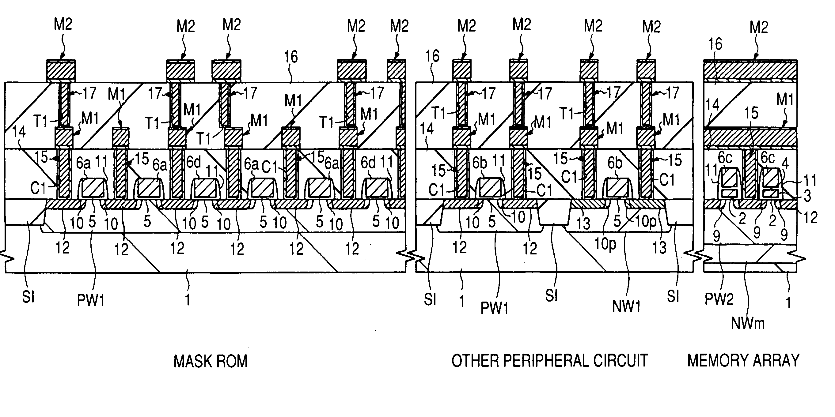
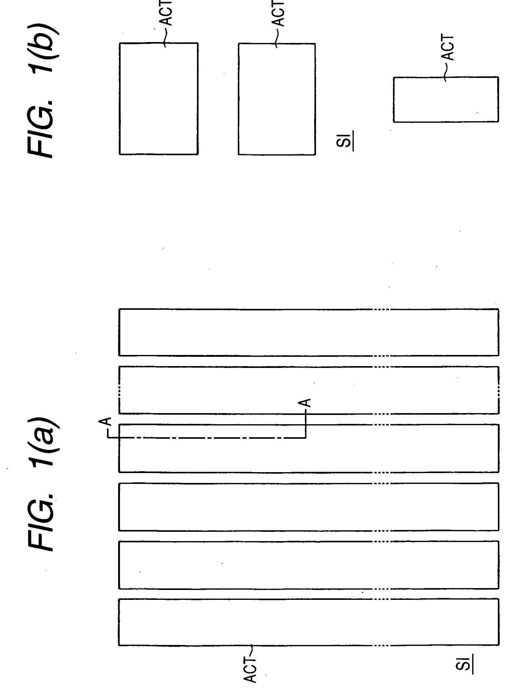
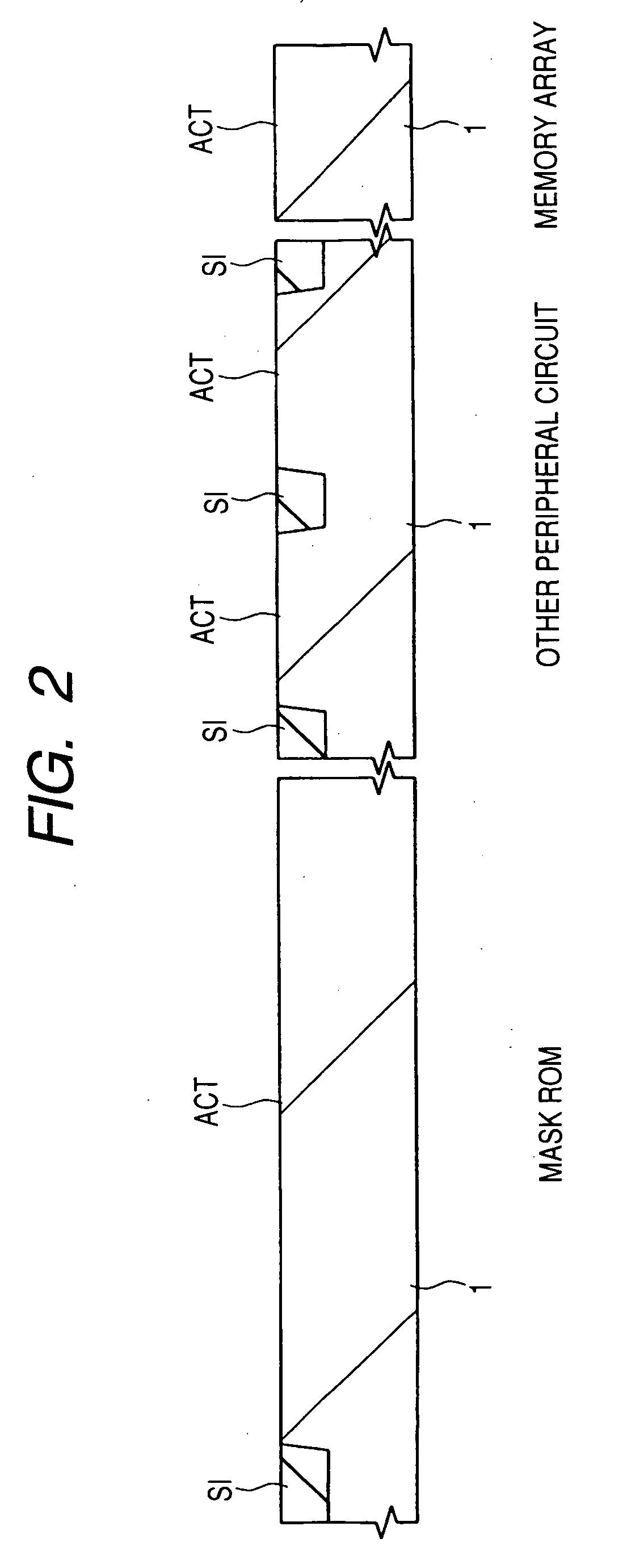
[0101]FIGS. 15 and 16 illustrate the flash memory of Embodiment 2 during its manufacturing step. FIG. 15(a) is a fragmentary plan view of a mask ROM region and FIG. 15(b) is a fragmentary plan view of the other peripheral circuit region. FIG. 16 is a fragmentary cross-sectional view including the mask ROM region, other peripheral circuit region and memory array, and in the mask ROM region, a fragmentary cross-sectional view taken along a line A-A of FIG. 15(a) is shown.

[0102] In the main surface of a semiconductor substrate 21 made of, for example, single crystal silicon, an isolation portion SI in the form of a trench and an active region ACT encompassed thereby are formed as in E...

embodiment 3

[0133] In Embodiment 2, different steps are employed for the formation of the isolation gate electrode in the second element isolation region of the mask ROM region and for the formation of the assist gate electrode, the local word line of the mask ROM region and the gate electrode of the other peripheral circuit region. In Embodiment 3, on the other hand, the isolation gate electrode, and the assist gate electrode and the gate electrode of the other peripheral circuit are formed in one step.

[0134] A manufacturing method of a flash memory according to Embodiment 3 will hereinafter be described in the order of steps based on FIGS. 30 to 38. Here, another application example of the present invention to a manufacturing method of an AND type flash memory having an assist gate will be described.

[0135] FIGS. 30(a), 30(b) and 31 illustrate the flash memory of Embodiment 3 during its manufacturing step. FIG. 30(a) is a fragmentary plan view of a mask ROM region and FIG. 30(b) is a fragmen...


PUM


Abstract

To improve reliability of FETs having element isolation regions for electrically isolating field effect transistors adjacent to each other in the gate length direction in a mask ROM region, the isolation regions are each constructed by field plate isolation formed simultaneously with gate electrodes of the field effect transistors. This relatively lessens a stress generated in an active region ACT sandwiched by the element isolation regions even if the isolation width of each element isolation region is made relatively small, specifically, less than 0.3 μm. It is therefore possible to relax or prevent the generation of crystal defects resulting from the stress, thereby reducing occurrence of an undesired leak current between the source and drain of each field effect transistor.

Description

CROSS-REFERENCE TO RELATED APPLICATION [0001] The present application claims priority from Japanese patent application No. 2004-356216 filed on Dec. 09, 2004, the content of which is hereby incorporated by reference into this application. BACKGROUND OF THE INVENTION [0002] The present invention relates to a semiconductor device and a manufacturing method of the same, in particular, to a technology effective when applied to the manufacture of a plurality of field effect transistors electrically isolated each other by an element isolation region having a width less than 0.3 μm. [0003] Shallow trench isolation (which will hereinafter be abbreviated as “STI”) is one of element isolation structures enabling electrical isolation of two adjacent semiconductor elements. The STI is a structure obtained by making a trench having, for example, a depth of approximately 0.4 μm in an element isolation region of a substrate and then filling an insulating film therein or has such a structure. [0004...

Claims


Application Information

Patent Timeline
Patent Type & Authority Applications(United States)
IPC IPC(8): H01L21/8234H01L29/76
CPCH01L21/823842H01L27/105H01L27/11293H01L27/11526H01L27/11546H10B20/65H10B41/40H10B41/49H01L21/76
Inventor ISHIGAKI, YOSHIYUKI
Owner RENESAS TECH CORP
Why Eureka
Try Eureka