Back-illuminated type solid-state imaging device

a solid-state imaging and backlighting technology, applied in the field of backlighting-type solid-state imaging devices, can solve the problems of difficult operation of electronic shutters simultaneously with respect to all pixels, and achieve the effects of less noise, improved sensitivity, and suppressing dark curren

Inactive Publication Date: 2006-06-15
SONY SEMICON SOLUTIONS CORP
View PDF4 Cites 69 Cited by
  • Summary
  • Abstract
  • Description
  • Claims
  • Application Information

AI Technical Summary

Benefits of technology

[0046] By forming the transfer transistor in the semiconductor substrate under the insulation film, the pixel can be formed to have one photoelectric conversion element and a plurality of transistors including the transfer transistor. In addition, by making the photoelectric conversion element formed into the buried type, the charge from the interface can be recombined and the dark current can be suppressed.
[0047] With the voltage to the rear surface electrode being made into the voltage of the first polarity and an electron multiplication being performed in the semiconductor substrate, a back-illuminated type solid-state imaging device which has less noise and improved sensitivity can be provided.
[0048] According to the method for manufacturing the back-illuminated type solid-state imaging device of the present invention, a back-illuminated type solid-state imaging device whose reliability is excellent can be manufactured in which the electric field to collect the signal charge generated in the above-described photoelectric conversion element can be generated reliably and the crosstalk to the adjacent pixels can be reduced, for example.

Problems solved by technology

Further, an electronic shutter operation is performed through a reset transistor in the CMOS solid-state imaging device of the back-illuminated type, and it has been difficult to operate an electronic shutter simultaneously with respect to all pixels.

Method used


Image

  • Back-illuminated type solid-state imaging device
  • Back-illuminated type solid-state imaging device
  • Back-illuminated type solid-state imaging device

Examples


first embodiment

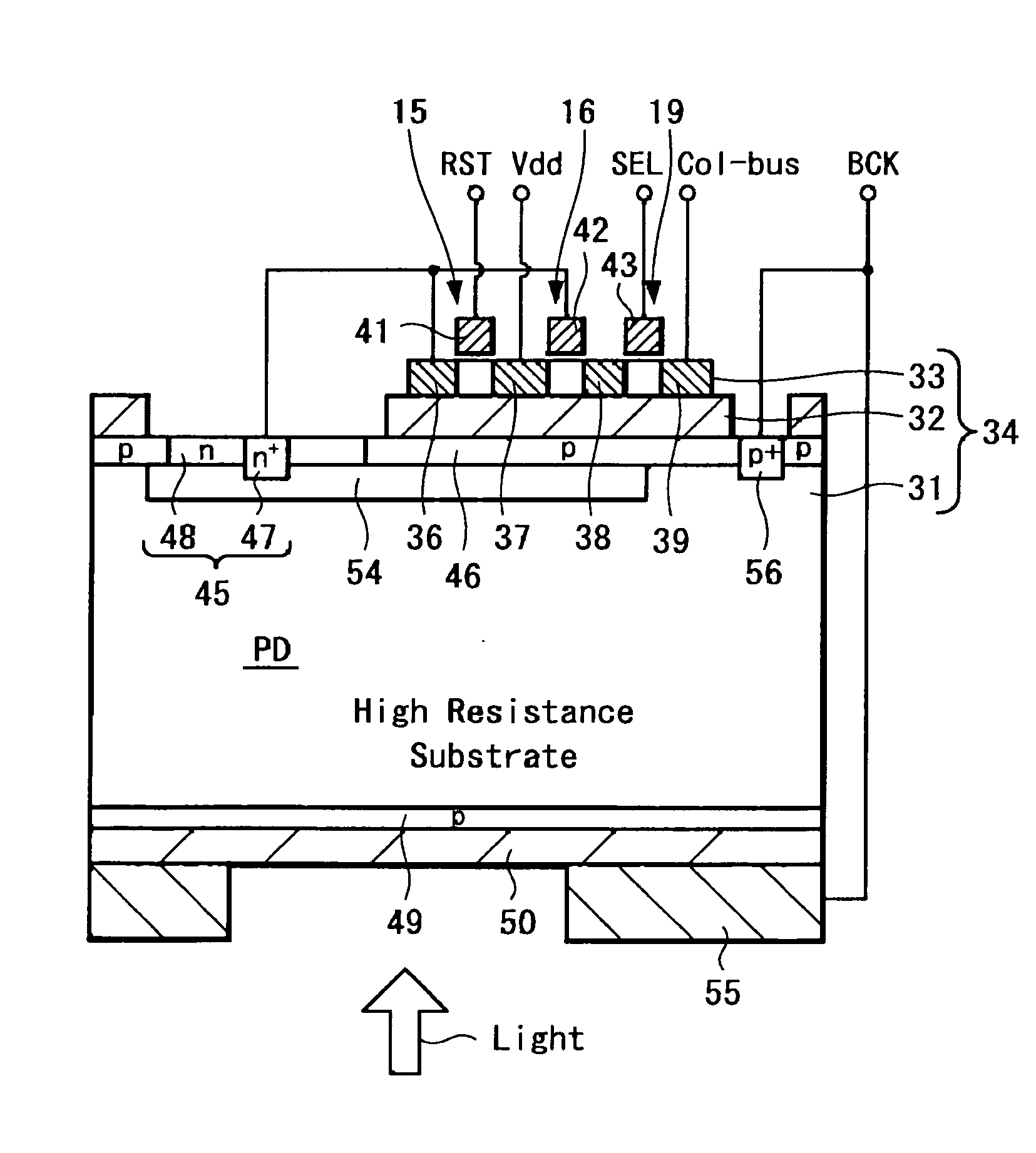
[0070]FIG. 3 shows a cross section of a relevant portion of a pixel in a CMOS solid-state imaging device according to the present invention. The CMOS solid-state imaging device of this embodiment includes what is called an SOI substrate 34 which has a silicon semiconductor film 33 provided on a silicon semiconductor substrate 31 through an insulation film 32 that is a buried silicon oxide film, for example.

[0071] In this embodiment, each of the reset transistor 15, amplifier transistor 16, and selector transistor 19 is formed in the semiconductor film 33 on the insulation film 32 of the SOI substrate 34. Specifically, the reset transistor 15 is formed with source-drain regions 36 and 37 of n-type that is a second conduction type formed in the semiconductor film 33 of p-type that is a first conduction type in this embodiment and a gate electrode 41 formed through a gate insulation film; the amplifier transistor 16 is formed with source-drain regions 37 and 38 of n-type and a gate ele...

second embodiment

[0083]FIG. 4 shows a cross section of a relevant portion of a pixel in a CMOS solid-state imaging device of a back-illuminated type according to the present invention. The CMOS solid-state imaging device of this embodiment has a structure of the above-described embodiment of FIG. 3, in which further an n− semiconductor region 54 whose impurity concentration is lower than the n-type semiconductor region 45 is formed extending on the front surface side of the substrate from part of the portion under the p-type semiconductor layer 46 to the portion under the n-type semiconductor region 45, the transparent electrode 51 on the rear surface side of the substrate is not provided and a rear surface electrode 55 that also serves as a light-shielding film to shield a boundary of pixels is formed on the electron injection preventive film 50 on the rear surface side of the substrate, and the same voltage as the rear surface electrode 55 is applied to the p semiconductor layer 46 on the front su...

third embodiment

[0112]FIG. 11 is a cross section showing a relevant portion of a pixel according to a CMOS solid-state imaging device of a back-illuminated type of the present invention. In this embodiment, a transfer transistor 91 is added to the side of the semiconductor film 33 of the SOI substrate 34. Specifically, the transfer transistor 91, reset transistor 15, selector transistor 19, and amplifier transistor 16 are formed in the semiconductor film 33. In this pixel, the high impurity concentration region 47 of the n-type semiconductor region 45 of the photodiode PD is connected to a source of the transfer transistor 91, and a drain of the transfer transistor 91 is connected to the source of the reset transistor 15. The floating diffusion FD that is a connection midpoint between the transfer transistor 91 and the reset transistor 15 is connected to the gate of the amplifier transistor 16. The source of the amplifier transistor 16 is connected to the vertical signal line, and the drain thereof...


PUM


Abstract

A back-illuminated type solid-state imaging device is provided in which an electric field to collect a signal charge (an electron, a hole and the like, for example) is reliably generated to reduce a crosstalk.
The back-illuminated type solid-state imaging device includes a structure 34 having a semiconductor film 33 on a semiconductor substrate 31 through an insulation film 32, in which a photoelectric conversion element PD that constitutes a pixel is formed in the semiconductor substrate 31, at least part of transistors 15, 16, and 19 that constitute the pixel is formed in the semiconductor film 33, and a rear surface electrode 51 to which a voltage is applied is formed on the rear surface side of the semiconductor substrate 31.

Description

CROSS REFERENCES TO RELATED APPLICATIONS [0001] The present invention contains subject matter related to Japanese Patent Application JP 2004-363580 filed in the Japanese Patent Office on Dec. 15, 2004, the entire contents of which being incorporated herein by reference. BACKGROUND OF THE INVENTION [0002] 1. Field of the Invention [0003] The present invention relates to a back-illuminated type solid-state imaging device, particularly, to a CMOS solid-state imaging device of a back-illuminated type and a method for manufacturing thereof. [0004] 2. Description of the Related Art [0005] In the past, a CMOS solid-state imaging device of a back-illuminated type in which light is made incident from the rear surface side of a substrate to improve efficiency in using light and to obtain high sensitivity has been proposed as a CMOS solid-state imaging device. This back-illuminated type CMOS solid-state imaging device has a structure in which a CMOS transistor that constitutes a pixel is forme...

Claims


Application Information

Patent Timeline
Patent Type & Authority Applications(United States)
IPC IPC(8): H01L31/00H01L27/146H04N5/335H04N5/353H04N5/359H04N5/369H04N5/374
CPCH01L27/14603H01L27/14643H01L31/18H01L27/1464H01L2224/48091H01L2224/48464H01L2224/73257H01L2924/00014H01L27/14636H01L2924/13091H01L2924/00H01L27/146
Inventor MABUCHI, KEIJI
Owner SONY SEMICON SOLUTIONS CORP
Why Eureka
Try Eureka