Polymeric conductor donor and transfer method

Active Publication Date: 2006-06-22
EASTMAN KODAK CO
View PDF55 Cites 29 Cited by
  • Summary
  • Abstract
  • Description
  • Claims
  • Application Information

AI Technical Summary

Benefits of technology

[0035] The invention provides a desirable transfer element and a transfer method to form conductive layers, especially those compris

Problems solved by technology

The high cost of the fabrication methods and the low flexibility of such electrodes, due to the brittleness of the inorganic ITO layer as well as the glass substrate, limit the range of potential applications.
Such methods that involve conventional lithographic techniques are cumbersome as they involve many steps and require the use of hazardous chemicals.
UV exposure of such layers produces a base that reduces the conductivity in the exposed areas.
Such photoablation processes are convenient, dry, one-step methods but the generation of debris may require a wet cleaning step and may contaminate the optics and mechanics of the laser device.
However, the polythiophene layers in these patents are non-conductive in nature.
Such an involved process may be difficult to practice for roll-to-roll production of a wide flexible plastic substrate.
As mentioned earlier, such processes are difficult to implement for roll-to-roll production of conductive coatings.
In the same patent application, a comparative example was created using a dispersion of poly(3,4 ethylene dioxythiophene)/polystyrene sulfonic acid which resulted in inferior coating properties.
However, the transparency vs. surface electrical

Method used


Image

  • Polymeric conductor donor and transfer method
  • Polymeric conductor donor and transfer method
  • Polymeric conductor donor and transfer method

Examples


examples

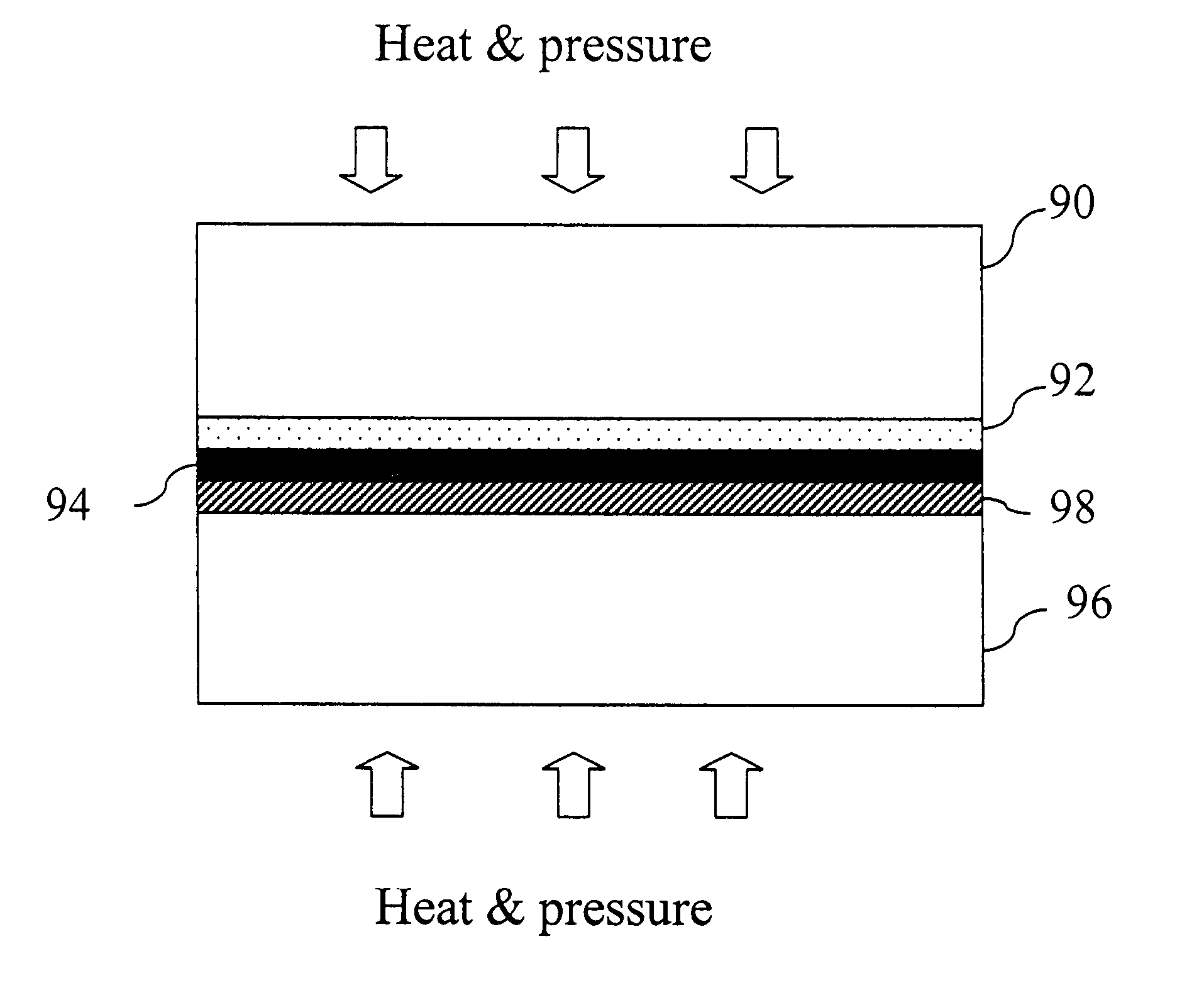
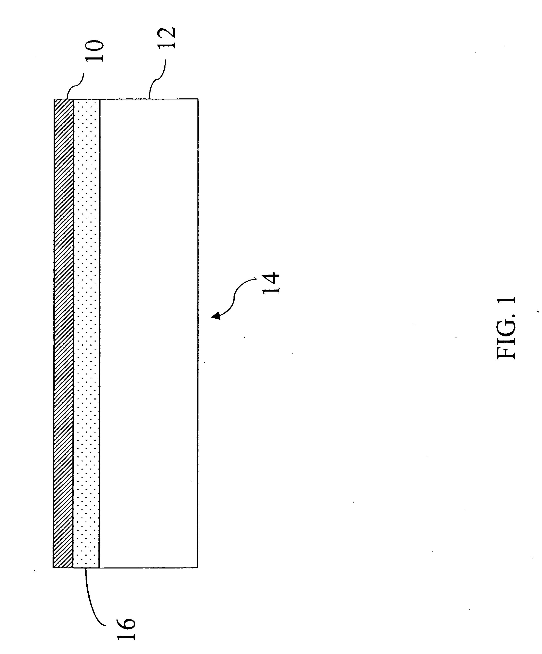
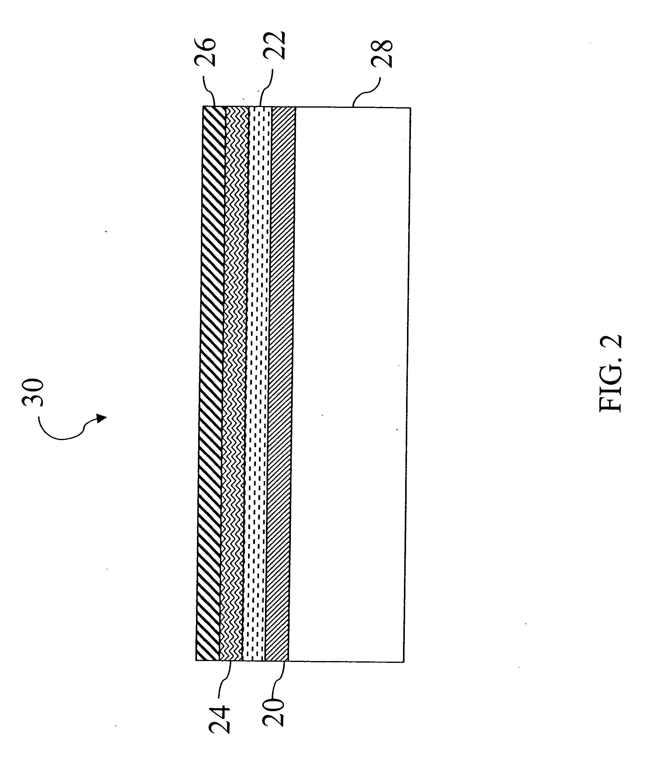
[0156] Donor Laminates

[0157] The donor laminates used in the following examples comprised of, a substrate, a silocone layer and a conductive coating, in the aforementioned order.

[0158] The substrate used was either polyethylene terephthalate (PET) or triacetylcellulose (TAC).

[0159] The silicone layer was either a solvent coated 3-glycidoxy-propyltrimethoxysilane layer (RL-1) or a thermally cured silicone layer commercially available from Rexam Corporation (RL-2).

[0160] The conductive coating was applied onto the silocone layer from a coating composition comprising the following ingredients: [0161] (a) Baytron P HC: aqueous dispersion of electronically conductive polythiophene and polyanion, namely, poly(3,4-ethylene dioxythiophene styrene sulfonate), supplied by H. C. Starck; [0162] (b) Olin 10G: nonionic surfactant supplied by Olin Chemicals; [0163] (c) N-methylpyrrolidone: conductivity enhancing agent supplied by Acros; [0164] (d) diethylene glycol: conductivity enhancing agen...


PUM

PropertyMeasurementUnit
Temperatureaaaaaaaaaa
Linear densityaaaaaaaaaa

Abstract

The present invention relates to a donor laminate for transfer of a conductive layer comprising at least one electronically conductive polymer on to a receiver, wherein the receiver is a component of a device. The present invention also relates to methods pertinent to such transfers.

Description

FIELD OF THE INVENTION [0001] The present invention relates to a donor laminate for transfer of a conductive layer comprising at least one electronically conductive polymer on to a receiver, wherein the receiver is a component of a device. The present invention also relates to methods pertinent to such transfers. BACKGROUND OF THE INVENTION [0002] Transparent electrically-conductive layers (TCL) of metal oxides such as indium tin oxide (ITO), antimony doped tin oxide, and cadmium stannate (cadmium tin oxide) are commonly used in the manufacture of electrooptical display devices such as liquid crystal display devices (LCDs), electroluminescent display devices, photocells, solid-state image sensors, electrochromic windows and the like. [0003] Devices such as flat panel displays, typically contain a substrate provided with an indium tin oxide (ITO) layer as a transparent electrode. The coating of ITO is carried out by vacuum sputtering methods which involve high substrate temperature c...

Claims


Application Information

Patent Timeline
IPC IPC(8): H01L23/58H01L21/44
CPCG02F1/13439H01L51/0022H01L51/0037H01L51/0097H01L51/5206H01L51/56H01L2251/5338H05K3/046H05K2201/0329H05K2203/0528H05K2203/107H10K71/611H10K85/1135H10K77/111H10K50/81H10K71/00H10K2102/311
Inventor MAJUMDAR, DEBASISIRVIN, GLEN C. JR.ANDERSON, CHARLES C.FREEDMAN, GARY S.KRESS, ROBERT J.
Owner EASTMAN KODAK CO
Why Eureka
Try Eureka