Hot-Melt Underfill Composition and Methos of Application

a technology of solvent-free underfill and composition, which is applied in the direction of basic electric elements, electrical apparatus, and semiconductor devices, can solve the problems of filler interference with soldering, time-consuming capillary and no flow underfill methods, and no flow assembly, etc., to achieve reduced cycle time, increase manufacturing efficiency, and high solder bump configuration

Inactive Publication Date: 2006-06-22
NAT STARCH & CHEM INVESTMENT HLDG CORP
View PDF0 Cites 38 Cited by
  • Summary
  • Abstract
  • Description
  • Claims
  • Application Information

AI Technical Summary

Benefits of technology

[0011] Inasmuch as no solvent is required, voiding or non-wets due to solvent outgassing during reflow are avoided. The underfill layer thickness can be any effective thickness as required for the particular process as determined by the practitioner. Thick layers of underfill can be used (>200 μm), if necessary, to accommodate higher solder bump configurations. There is significant reduction in cycle time, as any B-stage process can be very short. There is no need to process or dispose of solvent. The application is performed at the wafer level, increasing manufacturing efficiency compared with die-level underfill application. No new significant equipment infrastructure is required.

Problems solved by technology

No flow assembly can also be performed using thermocompression bonding.
Capillary and no flow underfill methods are time-consuming due to the fact that they are conducted at the die level.
Another major drawback of the no flow system is that if the no flow underfill is a filled system, then filler can interfere with soldering.
If the B-stage conditions are not optimized, residual solvent in the wafer level underfill can outgas during reflow, impeding good solder connections (leading to cold solder joints), or causing voids, which can lead potentially to failed devices, or causing areas that are not contacted by the underfill (non-wets).
Further, as the thickness of the underfill layer increases beyond 200 micrometers, removal of solvent from the underfill becomes very difficult.
The residual solvent outgases during reflow, causing voids and non-wets.

Method used


Image

  • Hot-Melt Underfill Composition and Methos of Application
  • Hot-Melt Underfill Composition and Methos of Application
  • Hot-Melt Underfill Composition and Methos of Application

Examples


example 1

[0073] The EXAMPLE 1 formulation was prepared using standard adhesive mixing techniques known to those skilled in the art, with the following composition:

Epon 1001F Bisphenol A / Epichlorohydrin Epoxy47.6 wt %Amorphous Silica Filler47.6 wt %Polysebacic Polyanhydride4.76 wt %

example 2

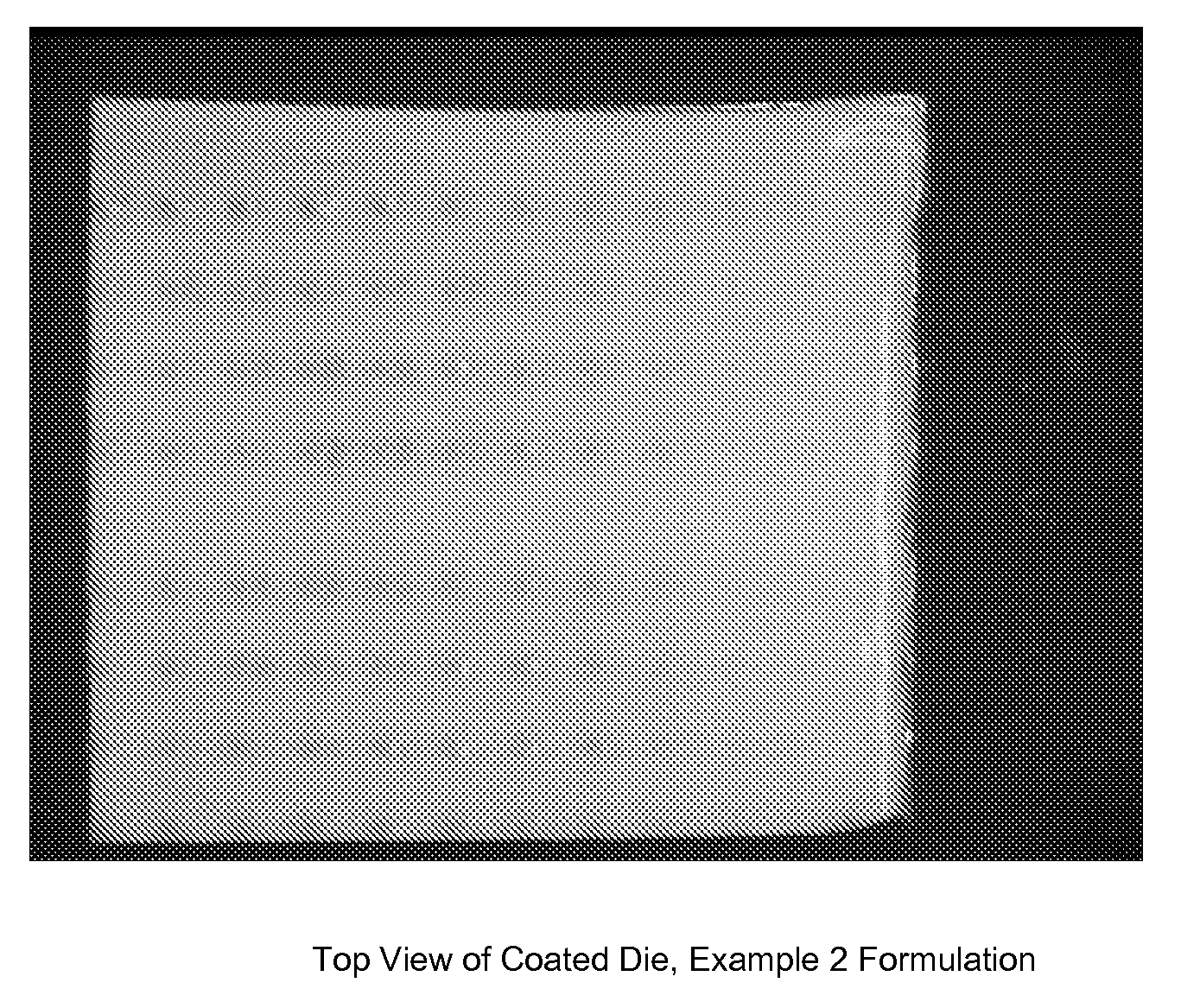
[0074] The EXAMPLE 2 formulation was prepared using standard adhesive mixing techniques known to those skilled in the art, with the following composition:

Epiclon HP-7200H Epoxy Resin41.7wt %Amorphous Silica Filler41.7wt %Dodecanedioic Acid Flux10.0wt %Epiclon 830S Bisphenol F Epoxy4.17wt %Hypox RM20 Rubber Modified Epoxy1.9wt %HRJ 1166 Novolac Phenol Resin0.48wt %Amino Aromatic Amide0.11wt %

[0075] Each composition was separately printed onto a silicon wafer that had 450 micron high bumps at 800 micron pitch. An aluminum stencil that was slightly thicker than the bumped wafer was used for printing, so that the material would fully cover the bumps. This ensured that the bumps were not damaged by the squeegee during printing. The wafer was placed inside the stencil on a hot plate. An excess amount of solid underfill was placed on the hot plate, at one end of the stencil and wafer. The stencil, wafer, and solid underfill were heated to 130° C., at which point the underfill was molten....


PUM


Abstract

This invention provides a process for applying a wafer level underfill comprising: providing a solvent-free hot-melt underfill composition; melting the underfill; applying the underfill in a uniform layer to the active side of a semiconductor wafer; returning the underfill to a solid state; optionally B-staging the underfill; optionally removing any excess underfill from the bumps on the wafer; and dicing the wafer into individual dies.

Description

FIELD OF THE INVENTION [0001] This invention relates to a hot-melt solvent-free underfill composition and the method of depositing that underfill, particularly onto a silicon semiconductor wafer before it is singulated into individual dies. BACKGROUND OF THE INVENTION [0002] In the construction of semiconductor assemblies, semiconductor dies or chips are both electrically and mechanically attached to substrates. In one method of attach, the face of the die containing electrical terminal pads and circuitry, the active face, is bumped with deposits of solder. These solder bumps are aligned and contacted with corresponding terminals on the substrate, the solder is heated to its melting point or “reflow” temperature to form solder joints, enabling mechanical support and electrical interconnections between the semiconductor die and the substrate. [0003] Differences between the coefficient of thermal expansion (CTE) of the die and the substrate often require that the space between the die...

Claims


Application Information

Patent Timeline
Patent Type & Authority Applications(United States)
IPC IPC(8): H01L21/44
CPCH01L21/563H01L2224/16H01L2224/274H01L2224/73203H01L2224/83191H01L2224/83856H01L2924/01005H01L2924/01013H01L2924/01015H01L2924/0102H01L2924/01025H01L2924/01027H01L2924/01029H01L2924/0103H01L2924/01032H01L2924/01033H01L2924/0104H01L2924/01047H01L2924/01049H01L2924/0105H01L2924/01056H01L2924/01074H01L2924/01075H01L2924/01079H01L2924/01082H01L2924/01322H01L2924/0132H01L24/29H01L2924/01006H01L2924/01023H01L2924/0133H01L2224/29111H01L2224/2919H01L2224/16225H01L2224/32225H01L2224/73104H01L2224/73204H01L2224/81191H01L2224/81193H01L2224/13111H01L2924/00014H01L2924/00H01L2224/94H01L2924/00011H01L2224/27H01L2224/11H01L2224/0401H01L21/20
Inventor CHAWARE, RAGHUNANDAN RAMESHHE, XIPINGSHENFIELD, DAVID
Owner NAT STARCH & CHEM INVESTMENT HLDG CORP
Why Eureka
Try Eureka