Semiconductor device and fabricating method of the same

a semiconductor and capacitor technology, applied in semiconductor devices, capacitors, electrical devices, etc., can solve the problems of preventing reliable electric connection, difficult to form connecting holes for establishing electric, and requiring relatively high voltage, so as to reduce poor contact, reduce poor resistance, and suppress degradation of capacitor characteristics.

Active Publication Date: 2006-06-29
FUJITSU SEMICON MEMORY SOLUTION LTD
View PDF9 Cites 6 Cited by
  • Summary
  • Abstract
  • Description
  • Claims
  • Application Information

AI Technical Summary

Benefits of technology

[0014] The present invention was made in view of the aforementioned problems and aims at providing a reliable semiconductor device and a fabricating method by sufficiently suppressing degradations of the characteristics of capacitor constructions and reducing poor contacts to improve the yield, while ensuring connections of electrically-connecting plugs.

Problems solved by technology

In order to write and erase information, it is necessary to pass tunnel currents through the insulating film, thus requiring relatively high voltages.
Therefore, it is difficult to form connecting holes for establishing electric contact with lower layers to be desired shapes.
For example, there is such problem that connecting holes are formed to be shapes having narrowed bottom portions, thus preventing the establishment of reliable electric connections.
However, when the technique of Patent Document 1 is employed, openings are formed in the protective film provided for suppressing degradations in the characteristics, which will necessarily degrade the blocking function of the protective film against hydrogen or process damages, making it difficult to sufficiently suppress degradations in the characteristics of the capacitor constructions.

Method used


Image

  • Semiconductor device and fabricating method of the same
  • Semiconductor device and fabricating method of the same
  • Semiconductor device and fabricating method of the same

Examples


first embodiment

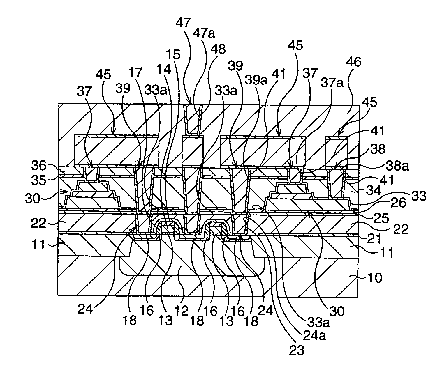
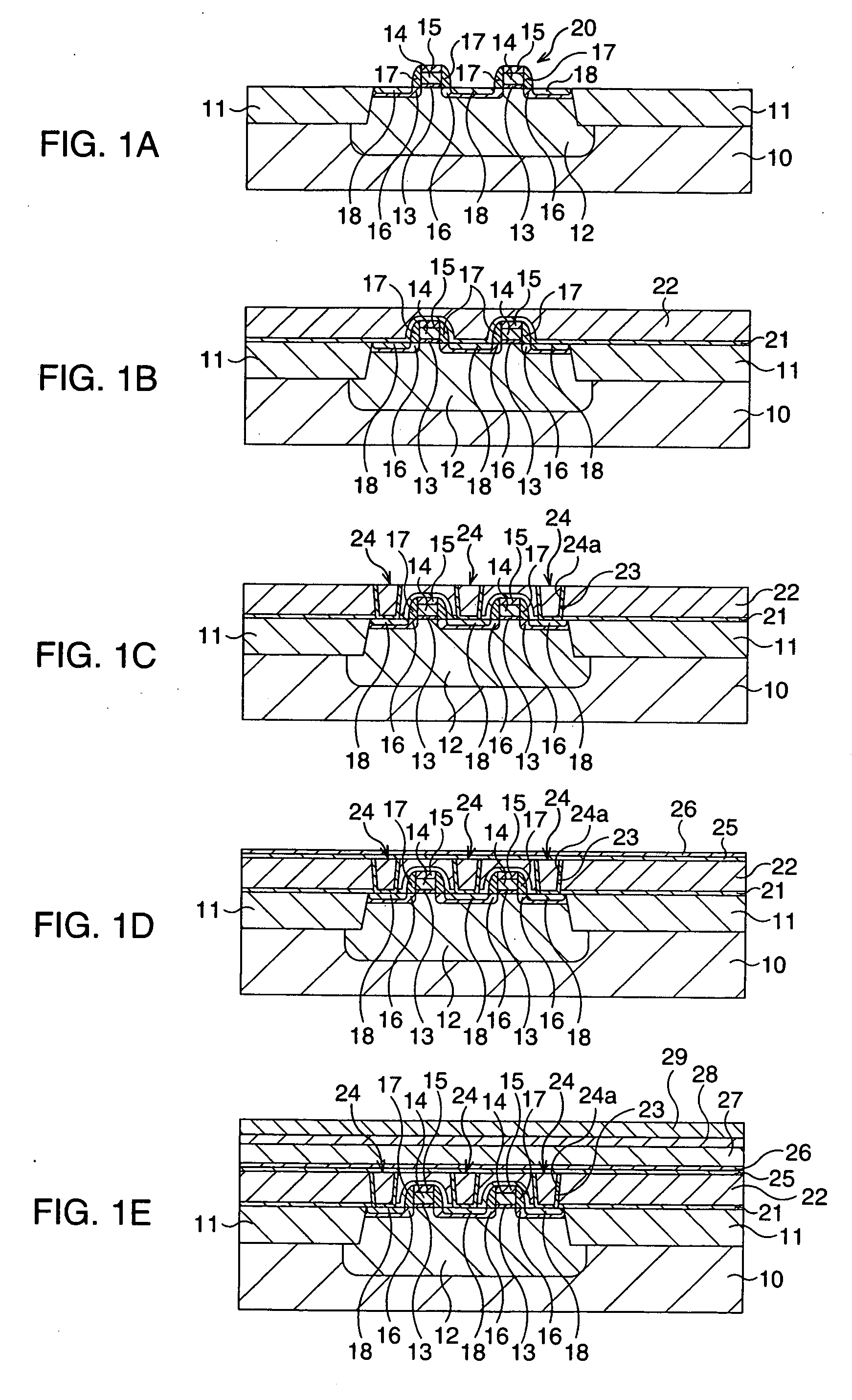
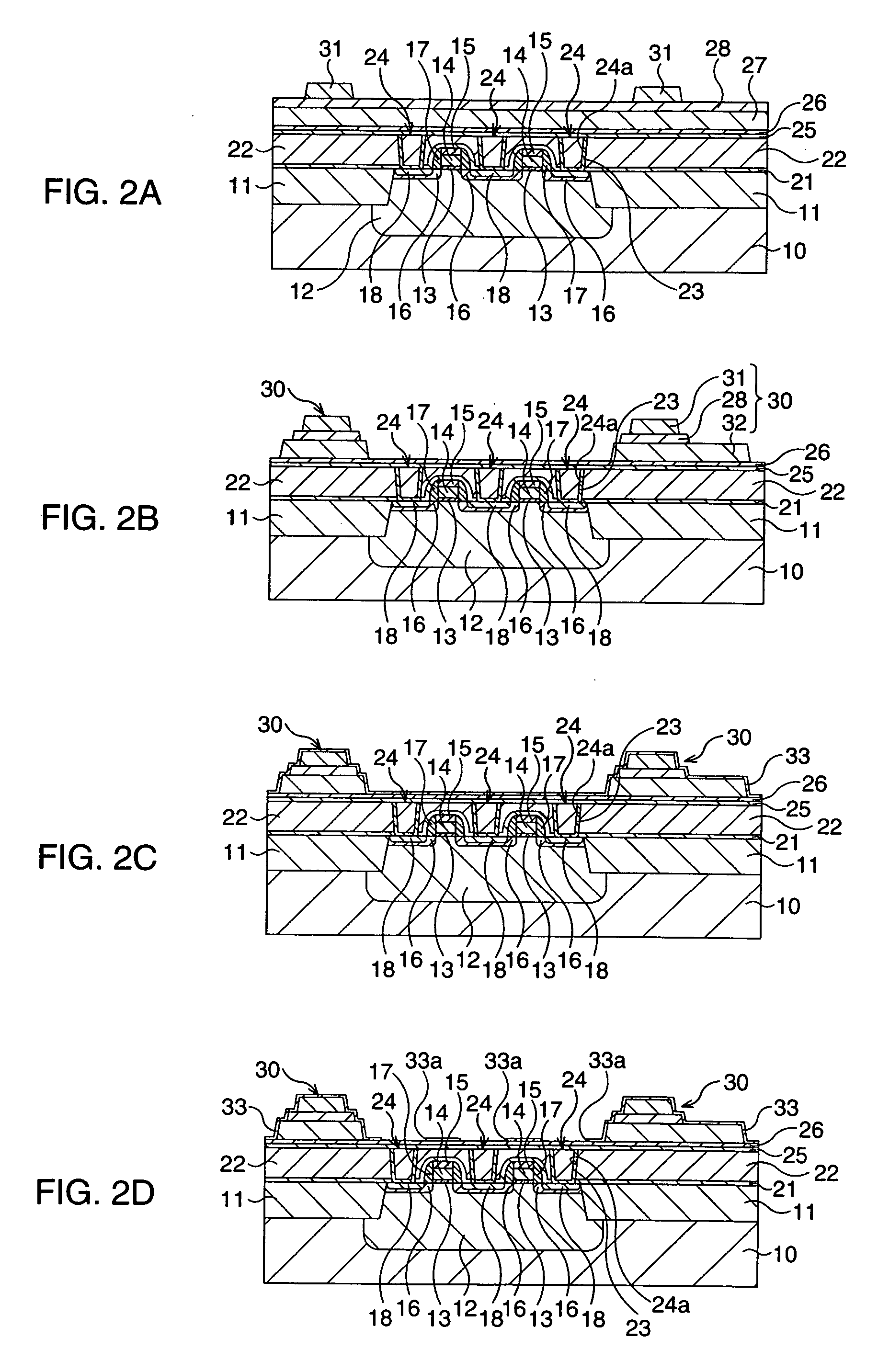
[0061]FIGS. 1A to 4B are schematic cross sectional views illustrating the fabricating method of a ferroelectric memory according to the present embodiment, in the order of the processes.

[0062] At first, as illustrated in FIG. 1A, MOS transistors 20 which function as selection transistors are formed on a silicon semiconductor substrate 10.

[0063] More specifically, a device separation construction 11 is formed by a STI (Shallow Trench Isolation) process, for example, on the surface layer of the silicon semiconductor substrate 10 to define a device activation region.

[0064] Subsequently, an impurity is implanted into the device activation region to form a well 12. In this case, B is implanted into the device activation region by ion implantation with a dose amount of 3.0×10¹³ / cm2 and an acceleration energy of 300 keV.

[0065] Then, a thin gate insulating film 13 with a thickness of about 3.0 nm is formed on the device activation region, for example, by thermal oxidation. Then, a polyc...

first modified embodiment

[0119]FIG. 10 is a cross sectional view for describing main processes of the present modified embodiment which are particularly different from those of the first embodiment.

[0120] In the present modified embodiment, similarly to in the first embodiment, firstly transistor constructions 20, first plugs 24, ferroelectric capacitor constructions 30 and a first protective film 33 are formed and, after the formation of them, the state of FIG. 10A corresponding to FIG. 2C is reached.

[0121] Subsequently, as illustrated in FIG. 10B, the first protective film 33 is processed.

[0122] More specifically, the first protective film 33 is processed by lithography and subsequent dry etching such that island-shaped portions of the first protective film 33 covering only the ferroelectric capacitor constructions 30 are left. At this time, the first protective film 33 is made to cover only the ferroelectric capacitor constructions 30 and the portions of the first protective film 33 lying over the fir...

second modified embodiment

[0133]FIG. 12 is a schematic cross sectional view for describing main processes of the second modified embodiment which are particularly different from those of the first embodiment.

[0134] In the present modified embodiment, similarly to in the first embodiment, firstly transistor constructions 20, first plugs 24, ferroelectric capacitor constructions 30 and a first protective film 33 are formed and, after the formation of them, the state of FIG. 12A corresponding to FIG. 2C is reached.

[0135] Subsequently, as illustrated in FIG. 12B, the first protective film 33 is processed.

[0136] More specifically, the first protective film 33 is processed by lithography and subsequent dry etching such that island-shaped portions of the first protective film 33 covering only the ferroelectric capacitor constructions 30 are left. At this time, the first protective film 33 is formed to have a size covering only the ferroelectric capacitor constructions 30, so to say, redundantly, namely a size on...


PUM


Abstract

Openings are formed by lithography and subsequent dry etching at the portions of a first protective film which correspond to connecting holes of second plugs which will be described later, namely at the portions thereof which align with first plugs, wherein the openings have a diameter greater than that of connecting holes by about 0.4 μm.

Description

CROSS-REFERENCE TO RELATED APPLICATIONS [0001] This is a continuation-in-part application of application Ser. No. 11 / 093,242, filed Mar. 30, 2005. [0002] This application is based upon and claims the benefit of priority from the prior Japanese Patent Application Nos. 2004-351905, filed on Dec. 3, 2004 and 2005-272595, filed on Sep. 20, 2005 the entire contents of which are incorporated herein by reference.BACKGROUND OF THE INVENTION [0003] 1. Field of the Invention [0004] The present invention relates to a semiconductor device including a capacitor construction consisting of a lower electrode, an upper electrode and a dielectric film interposed therebetween and a fabricating method of such a semiconductor device. [0005] 2. Description of the Related Art [0006] Conventionally, there are known flash memories and ferro-electric random access memories (FeRAMs) as nonvolatile memories which do not erase stored information even when the power supply is turned off. [0007] A flash memory in...

Claims


Application Information

Patent Timeline
Patent Type & Authority Applications(United States)
IPC IPC(8): H01L29/94H01L21/8242
CPCH01L21/76816H01L21/76829H01L27/11502H01L27/11507H01L28/65H01L21/76879H01L28/40H10B53/30H10B53/00H01L27/105
Inventor OZAKI, YASUTAKA
Owner FUJITSU SEMICON MEMORY SOLUTION LTD
Why Eureka
Try Eureka