OLEDs with improved operational lifetime

a technology of operating lifetime and oled, which is applied in the direction of discharge tube luminescnet screen, transportation and packaging, natural mineral layered products, etc., can solve the problems of insufficient lifetime and persisting low operational lifetime, and achieve the effect of improving the efficiency of oleds without adversely reducing the purity of color of emitted ligh

Inactive Publication Date: 2006-06-29
EASTMAN KODAK CO
View PDF24 Cites 127 Cited by
  • Summary
  • Abstract
  • Description
  • Claims
  • Application Information

AI Technical Summary

Benefits of technology

[0028] An advantage of the present invention is that it provides OLED devices suitable for long-life displays and lighting applications.
[0029] Another advantage of the present invention is that the OLED efficiency is improved without adversely reducing the purity of color of the emitted light.

Problems solved by technology

Although EL efficiency, color, and lifetime have been improved significantly using doped light-emitting layers of various compositions, the problem of low operational lifetime persists.
Insufficient lifetime presents the greatest obstacle for many desirable practical applications.

Method used


Image

  • OLEDs with improved operational lifetime
  • OLEDs with improved operational lifetime
  • OLEDs with improved operational lifetime

Examples


examples t1-t8

Test Devices

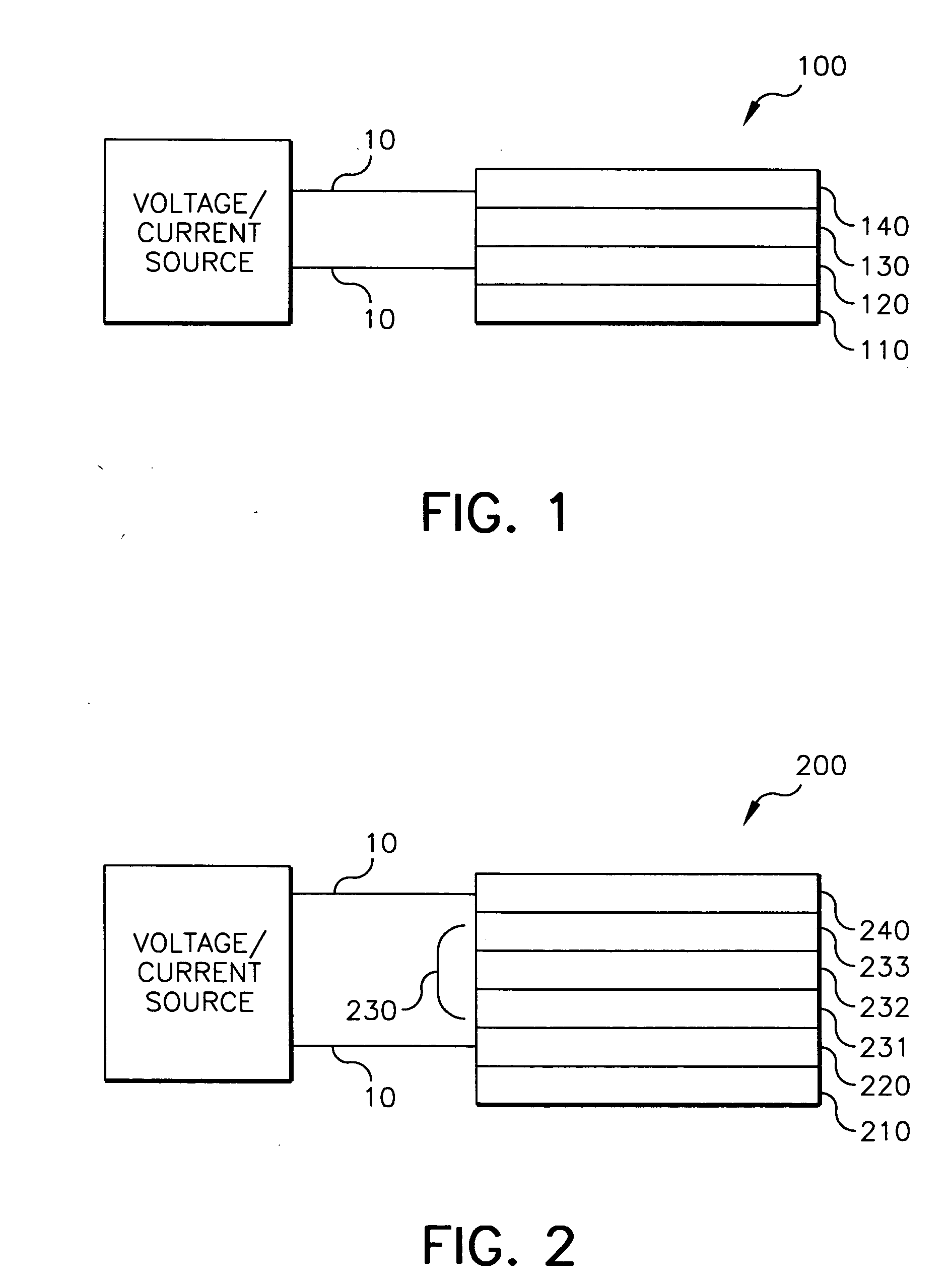
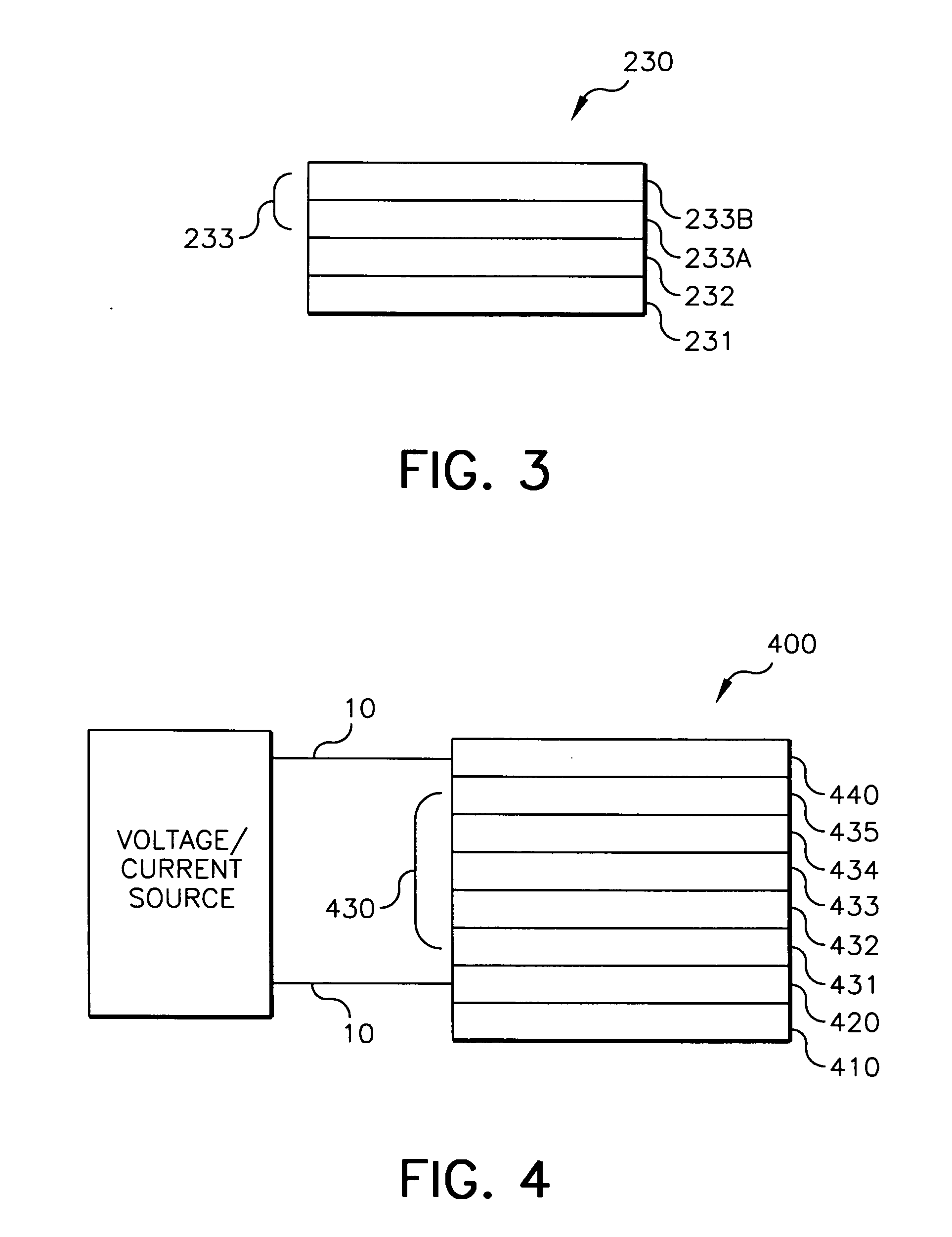
[0346] OLED devices T1-T8 (Table T1) were prepared as follows. A glass substrate coated with ˜250 Å transparent indium-tin-oxide (ITO) conductive layer was cleaned and dried using a commercial glass scrubber tool. The ITO surface was subsequently treated with oxygen plasma to condition the surface as an anode. Over the ITO was deposited a ˜10 Å thick hole-injecting layer of fluorocarbon (CFx) by plasma-assisted deposition of CHF3. The following layers were deposited in the following sequence by sublimation from heated crucible boats in a conventional vacuum deposition chamber under a vacuum of approximately 10−6 Torr (Table T1): [0347] (1) the HTL, 750 Å thick, composed of NPB; [0348] (2) the light-emitting layer, 375 Å thick, composed of AlQ; [0349] (3) the ETL, 375 Å thick, composed of either AlQ (reference device T1), AlQ doped with 3.7% Li, or a test ETL material, which is either undoped or doped with 3.7% Li; [0350] (4) the cathode, 2,100 Å thick, including an allo...

example 1 (

Device Example 1 (Inventive)

[0355] An OLED device (Device 1) was prepared as follows. A glass substrate was coated with about an 850 Å transparent indium-tin-oxide (ITO) conductive layer and was cleaned and dried using a commercial glass scrubber tool. The ITO surface was subsequently treated with an oxidative plasma to condition the surface as an anode. Over the ITO was deposited a 10 Å thick hole-injecting layer of fluorocarbon (CFx) by plasma-assisted deposition of CHF3. The following layers were deposited in the following sequence by thermal evaporation from heated crucible boats in a conventional vacuum deposition chamber under a vacuum of approximately 10−6 Torr: (1) a hole-transporting layer, 750 Å thick, including NPB; (2) a light-emitting layer, 600 Å thick, including the first host Dibenzo[b,k]perylene (DBP) (32.5 volume %) and the second host component, Alq3 (66.5 volume %) and containing 1.0 volume % light-emitting dopant DCJTB; (3) an electron-transporting layer (ETL), ...

example 2 (comparative)

Device Example 2 (Comparative)

[0356] An OLED comparative device (Device 2) was prepared in the same manner as Device 1, except the ETL did not contain Li.


PUM

PropertyMeasurementUnit
optical densityaaaaaaaaaa
voltageaaaaaaaaaa
voltageaaaaaaaaaa

Abstract

An organic light-emitting device includes a substrate, an anode and a cathode disposed over the substrate, and a light-emitting layer disposed between the anode and the cathode wherein the light-emitting layer includes a host and at least one dopant. The host of the light-emitting layer is selected to include a solid organic material including a mixture of at least two components wherein the first host component is an organic compound capable of transporting electrical charges and also forms an aggregate, and the second component of the mixture is an organic compound capable, of transporting electrical charges and, upon mixing with the first host component, is capable of forming a continuous and substantially pin-hole-free layer. The dopant of the light-emitting layer is selected to collect excitons and produce colored light, and an electron-transporting layer is disposed between the light-emitting layer and the cathode for providing improved electron injection and transport.

Description

CROSS REFERENCE TO RELATED APPLICATIONS [0001] This application is a continuation-in-part of commonly-assigned U.S. patent application Ser. No. 10 / 921,603 filed Aug. 19, 2004. Reference is made to commonly assigned U.S. patent application Ser. No. 10 / 690,940 filed Oct. 22, 2003 by Tukaram K. Hatwar, et al., entitled “A Stabilized White-Light-Emitting OLED Device”; the disclosure of which is herein incorporated by reference.FIELD OF THE INVENTION [0002] The present invention relates to organic light-emitting diode devices and more particularly to the design of the composition of the organic layers for improvements in operational lifetime. BACKGROUND OF THE INVENTION [0003] Organic light-emitting diodes (OLED), also known as organic electroluminescent (EL) devices, are a class of electronic devices that emit light in response to an electrical current applied to the device. The structure of an OLED device generally includes an anode, an organic EL medium, and a cathode. The term, organ...

Claims


Application Information

Patent Timeline
Patent Type & Authority Applications(United States)
IPC IPC(8): H01L51/54H05B33/12
CPCC09K11/06Y10T428/24942C09K2211/1029C09K2211/1033C09K2211/1037C09K2211/1055C09K2211/1059C09K2211/1088H01L51/0052H01L51/0059H01L51/0062H01L51/0081H01L51/5012H01L51/5048H05B33/14C09K2211/1011H10K85/649H10K85/615H10K85/631H10K85/324H10K50/14H10K50/11
Inventor KLUBEK, KEVIN P.JARIKOV, VIKTOR V.LIAO, LIANG-SHENGBROWN, CHRISTOPHER T.TANG, CHING W.
Owner EASTMAN KODAK CO
Why Eureka
Try Eureka