
Photoresist formulation for high aspect ratio plating

a technology of high aspect ratio and mask, applied in the field can solve the problems of increasing so as to improve the adhesion of the mask, reduce the cost of ic devices, and improve the effect of high aspect ratio lithography

Inactive Publication Date: 2006-06-29
FORMFACTOR INC
View PDF17 Cites 3 Cited by
  • Summary
  • Abstract
  • Description
  • Claims
  • Application Information

AI Technical Summary

Benefits of technology

The modified photoresist composition demonstrates improved adhesion and reduced film stress, enhancing the viability of larger wafers by increasing the shear force and reducing via cracking frequency, thus supporting the production of more complex semiconductor devices.

Problems solved by technology

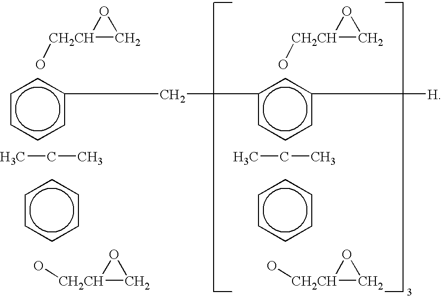
While the SU-8 family of photoresist materials enjoys relatively wide use and positive results as a photoresist in IC lithography, its utility is somewhat limited for use with silicon wafers greater than three or four inches in diameter.
As with most polymer photoresists, the SU-8 family of photoresist materials is prone to delamination and via cracking arising from high film stress when used with relatively large silicon wafers.
Another problem with the SU-8 family of photoresists arises from adhesion problems with certain substrate materials.
The IC device industry is constantly demanding larger and / or more complex devices.

Method used


Image

  • Photoresist formulation for high aspect ratio plating
  • Photoresist formulation for high aspect ratio plating

Examples


example 1

Preparation of Unmodified SU-8 Masking Composition

[0038] A two-step process is used to produce SU-8 photoresist without adhesion and plasticity modification.

[0039] Stock Solution. In a 2 L mixing container equipped with a mechanical stirrer or roller add 624 g of solid Epon SU-8 resin and 262 g of Gama-butyrolactone. The mixture is allowed to soak with occasional agitation until a viscous homogeneous solution is formed. This is a slow dissolution process and may take between 1-5 days to complete. The process can be accelerated by heating to about 60° C. if needed. Make sure the container is properly sealed during the process so that water absorption is kept to a minimum.

[0040] The solution then can be filtered through a 5 μm filter at room or elevated temperature to ensure gel-free resin stock solution. The above operation can be performed under normal lighting.

[0041] Final mixture. To 886 g of the resin stock solution under yellow light, add 63 g of filtered Cyracure® 6974 and ...

example 2

Preparation of Modified SU-8 Masking Composition

[0042] A two-step mixing process is also used to produce the modified GD41 solution:

[0043] Stock Solution. In a 2 L mixing container equipped with a mechanical stirrer or roller add 624 g of solid Epon SU-8 resin, 262 g of Gama-butyrolactone, and a 10 g of dioctyl phthalate (DOP). The mixture is allowed to soak with occasional agitation until a viscous homogeneous solution is formed. This is a slow dissolution process and may take between 1-5 days to complete. The process can be accelerated by heating to about 60° C. if needed. Make sure the container is properly sealed during the process so that water absorption is kept to a minimum. The solution is then filtered through a 5 μm filter at room or elevated temperature to ensure gel-free resin stock solution. The above operation can be performed under normal lighting.

[0044] Final mixture. To 896 g of resin stock solution under yellow light, add 64 g of filtered Cyracure® 6974 and mix ...

example 3

Preparation of Alternative Modified SU-8 Masking Composition

[0045] A photoresist composition was made by combining the following components with mixing: 62.4% SU-8 resin, 26.3% γ-butyrolactone, 6.3% Cyracure® 6974, 1% DOP, and 4% GPTMS, all on a weight percent basis. The photoresist was prepared under yellow light, stored in an opaque container, and allowed to debubble. The coating was applied to copper seed silicon wafers, was dried, exposed, and submitted to a PEB to provide a photoresist film with superior adhesion and film stress properties.


PUM

PropertyMeasurementUnit
boiling pointaaaaaaaaaa

Abstract

SU-8 photoresist compositions are modified to improve their adhesion properties by adding 1% to 6% of an adhesion promoter selected from the group consisting of glycidoxypropanetrimethoxysilane, mercatopropyltrimethoxysilane, and aminopropyltrimethoxysilane. SU-8 photoresist compositions are modified to improve their resistance to cracking and film stress by adding 0.5% to 3% of a plasticizer selected from the group consisting of dialkylphthalates, dialkylmalonates, dialkylsebacates, dialkyladipates, and diglycidyl hexahydrophthalates. The improvements can be obtained simultaneously by adding both the adhesion promoter and the plasticizer to SU-8 photoresist compositions.

Description

FIELD OF THE INVENTION [0001] The present invention relates generally to photoresist masks for high aspect ratio plating on semiconductor circuit boards, and more particularly to improvements in negative photoresist masks made from octafunctional epoxidized novolac resins such as SU-8. BACKGROUND OF THE INVENTION [0002] Negative photoresist masks are commonly employed in lithographic processes used to build integrated circuit boards. As is known in the art, lithography is a process by which geometric shapes are transferred from a mask onto the surface of a substrate. These geometric shapes, when transferred onto the surface of a silicon wafer, make up the parts of the circuit, such as gate electrodes, contact windows, probe electrodes, switches, metal interconnections, and the like. [0003] The steps of the lithographic process are generally as follows. First, a base semiconductor (e.g., silicon) substrate is provided, and a second material layer, such as an oxide layer, is formed th...

Claims


Application Information

Patent Timeline
Patent Type & Authority Applications(United States)
IPC IPC(8): G03C1/76G03F7/038G03F7/075G03F7/085
CPCG03F7/0385G03F7/0751G03F7/085Y10S430/128Y10S430/113Y10S430/155
Inventor FANG, TRELIANT
Owner FORMFACTOR INC
Learn More