Biomolecule detecting element and method for analyzing nucleic acid using the same

Inactive Publication Date: 2006-06-29
NAT INST FOR MATERIALS SCI
View PDF7 Cites 193 Cited by
  • Summary
  • Abstract
  • Description
  • Claims
  • Application Information

AI Technical Summary

Benefits of technology

[0032] The biomolecule detecting element of the invention does not require expensive lasers or complex optical detection systems. Because the biomolecule detecting element of the invention is based on the detection of surface potentials in a steady state, as opposed to the current detect

Problems solved by technology

However, many of the existing DNA chips or DNA microarrays are based on the detection of fluorescence as a basic princip

Method used


Image

  • Biomolecule detecting element and method for analyzing nucleic acid using the same
  • Biomolecule detecting element and method for analyzing nucleic acid using the same
  • Biomolecule detecting element and method for analyzing nucleic acid using the same

Examples


embodiment 1

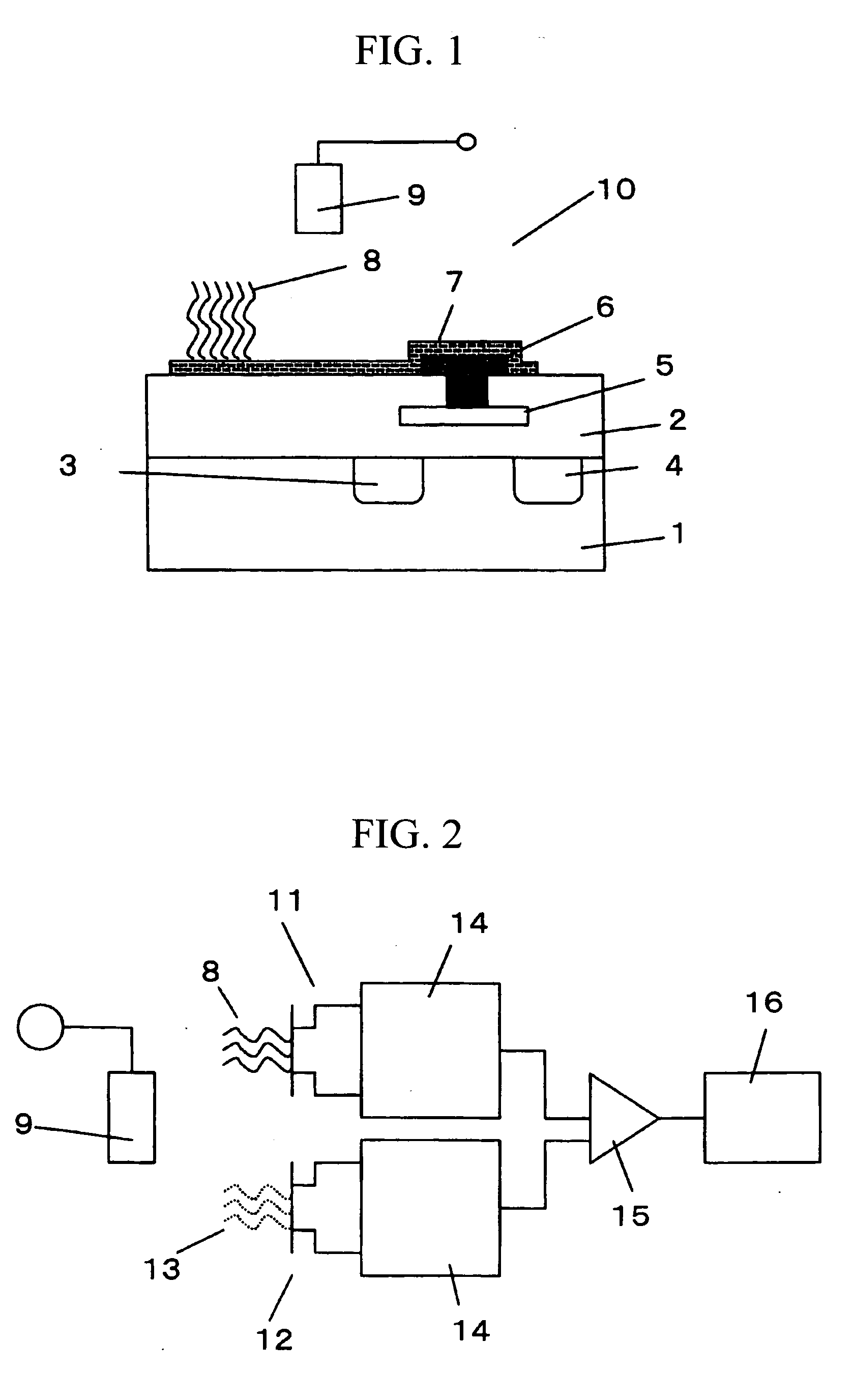
[0041]FIG. 1 schematically shows a cross section of a biomolecule detecting element (biomolecule detecting transistor) according to the invention.

[0042] An insulated gate field effect transistor is produced by forming a gate insulating film 2, a source 3, and a drain 4 on the surface of a silicon substrate 1, and providing a gate electrode 5 on the gate insulating film between the source and drain. On the surface of the gate electrode 5 is further formed an insulating film, such that the gate electrode 5 is embedded in the insulating film 2. A throughhole is formed in the insulating film 2, and a lead-out electrode 6 is formed using a conductive material and is placed in an electrical contact with the gate electrode 5. A floating electrode 7 is further formed on the surface of the gate insulating film and is placed in electrical contact with the lead-out electrode 6. A DNA probe 8 is immobilized on the surface of the floating electrode 7. The thus produced gene transistor is immers...

embodiment 2

[0056]FIG. 2 schematically shows a gene examination system in which the biomolecule detecting transistor according to the first embodiment is used. In this system, a reference transistor 12 is used in addition to the biomolecule detecting transistor 11 shown in FIG. 1, and a differential measurement is carried out using the two transistors.

[0057] On the surface of the gate of the biomolecule detecting transistor, a DNA probe 8 having a base sequence complementary to that of the target gene in the sample is immobilized. On the other hand, on the surface of the gate of the reference transistor, a DNA probe 13 having a base sequence different from the complementary base sequence of the target gene is immobilized. To stably measure the surface potential of the biomolecule detecting transistor and the reference transistor, a reference electrode 9 as a reference for potential measurement is provided. The surface potential of the biomolecule detecting transistor and that of the reference ...

embodiment 3

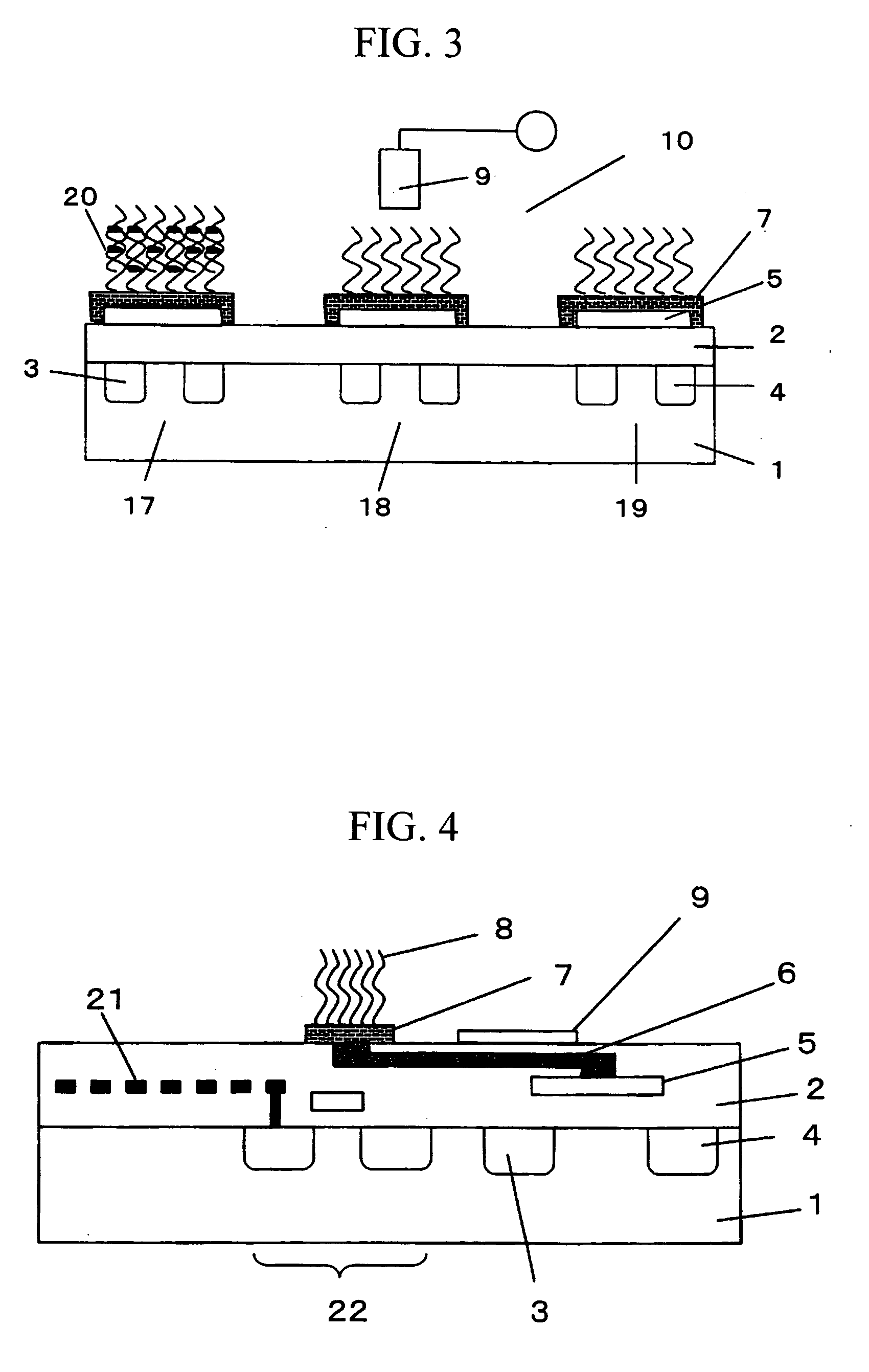
[0060]FIG. 3 schematically shows a cross section of another example of a measurement system employing the biomolecule detecting transistor shown in FIG. 1. In this measurement system, three FETs are integrated. A first biomolecule detecting transistor 17 is used for detecting a first target gene. A second transistor 18 is used for detecting a second target gene. A third transistor 19 is used as the reference transistor. On the gate electrode of the first and second biomolecule detecting transistors, a DNA probe having a base sequence complementary to that of the first and the second gene, respectively, is immobilized. On the surface of the gate electrode of the reference FET, a DNA probe having a base sequence different from the complementary base sequence of the first or second gene is immobilized.

[0061] The state shown in FIG. 3 is that where a sample solution containing only the first gene has been introduced into the aforementioned integrated transistors and hybridized to the t...


PUM

PropertyMeasurementUnit
Densityaaaaaaaaaa

Abstract

An inexpensive DNA chip/DNA microarray system capable of highly accurate measurement with low running cost. A DNA probe 8 is immobilized on a floating electrode 7 connected to a gate electrode 5 of a field effect transistor. Hybridization with a target gene is carried out on the surface of the floating electrode, when a change in surface charge density is detected using a field effect.

Description

TECHNICAL FIELD [0001] The present invention relates to biotechnology, particularly technologies in the field of genetic examination, such as genetic diagnosis, DNA sequencing analysis, and gene polymorphism analysis. In particular, the invention relates to a biomolecule detecting element suitable for accurately analyzing a plurality of different nucleic acids in parallel, and to a method for analyzing nucleic acids employing the element. BACKGROUND ART [0002] With the rapid increase in the rate at which the genome sequences of various living organisms, such as the human genome, are read, vast amounts of base sequence data have been accumulated. It is expected that from now on, gene functions in living organisms will be clarified and a significant progress will be made in gene-related technologies in a wide array of fields, such as in the diagnosis of a variety of diseases, development of drugs, and improvements in agricultural product varieties. These developments in new fields wil...

Claims


Application Information

Patent Timeline
IPC IPC(8): C12Q1/68C12M1/34C12M1/00G01N33/53G01N27/00G01N27/414G01N33/543G01N37/00
CPCB01J2219/00529B01J2219/00608B01J2219/00612B01J2219/00626B01J2219/00637B01J2219/00653C12Q1/6837C12Q2565/607C12Q2563/173G01N27/4145
Inventor MIYAHARA, YUJISAKATA, TOSHIYAKAMAHORI, MASAOYAZAWA, YOSHIAKI
Owner NAT INST FOR MATERIALS SCI
Why Eureka
Try Eureka