Nitride based semiconductor light emitting device

a light emitting device and nitride technology, applied in the direction of valve housings, engine components, mechanical equipment, etc., can solve the problems of low light extraction efficiency, low light extraction efficiency of only 6%, and difficulty in providing sapphire substrates with rough surfaces, so as to improve the light extraction efficiency of the light emitting device

Inactive Publication Date: 2006-07-06
SAMSUNG ELECTRO MECHANICS CO LTD
View PDF11 Cites 127 Cited by
  • Summary
  • Abstract
  • Description
  • Claims
  • Application Information

AI Technical Summary

Benefits of technology

[0023] Differently from the prior art that a roughened pattern is directly formed at a sapphire substrate having a high hardness or at other nitride semiconductor regions, the present invention suggests that a light-permeable insulating material is deposited on at least one surface of a light emitting device to form an insulating layer, and a roughened pattern is formed at the insulating layer, thereby achieving a light-scattering layer to improve light extra...

Problems solved by technology

As a result, much of light, coming from active layers, shows total internal reflection, thereby being propagated in an undesired direction or being completely reflected and dissipated, resulting in only low light extraction efficiency.
More specifically, in nitride-based semiconductor light emitting devices where refraction index of a GaN layer is 2.4, light coming from active layers causes total internal reflection if its incidence angle is larger than 23.6° that is a critical angle at an GaN/air interface, thereby being propagated laterally to be dissipated or being propagated in an undesired direction, resulting in low light extraction efficiency of only 6%.
However, due to the fact that substrates, usually employed f...

Method used


Image

  • Nitride based semiconductor light emitting device
  • Nitride based semiconductor light emitting device
  • Nitride based semiconductor light emitting device

Examples


Embodiment Construction

[0031] Now, preferred exemplary embodiments of the present invention will be explained in more detail with reference to the accompanying drawings.

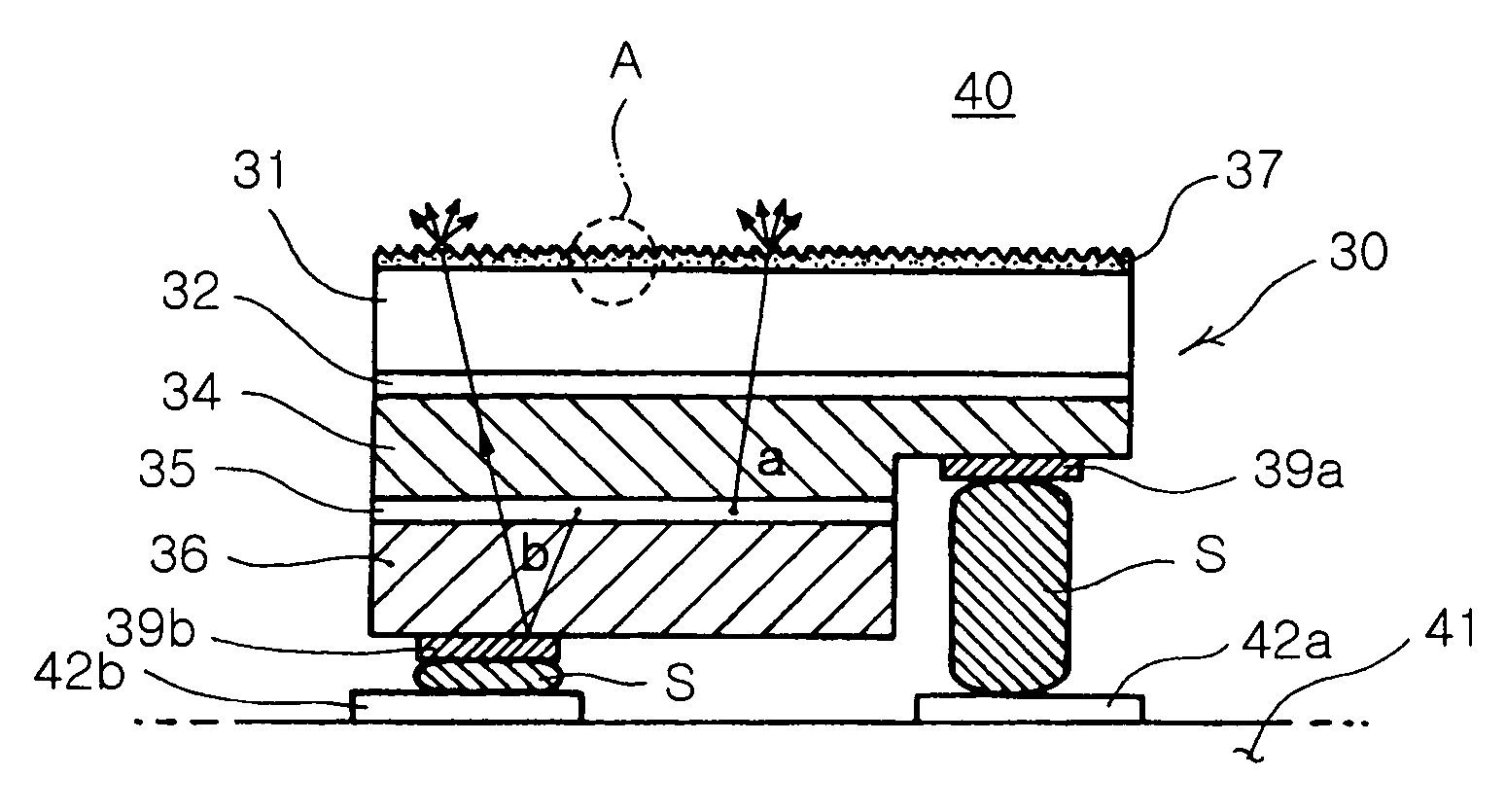
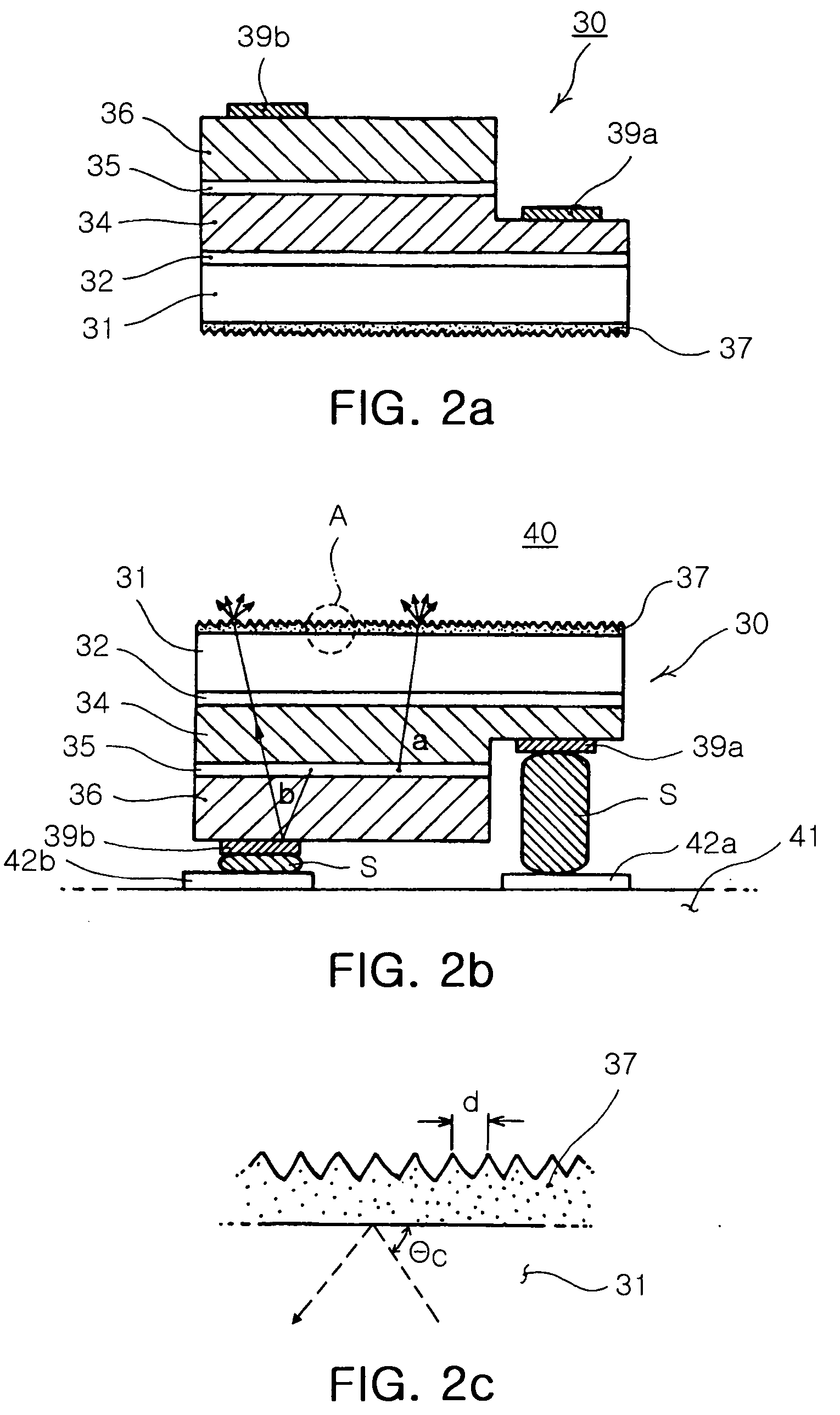
[0032]FIG. 2a is a side sectional view of a nitride-based semiconductor light emitting device in accordance with a first exemplary embodiment of the present invention. It can be understood that the nitride-based semiconductor light emitting device shown in FIG. 2a is employed in a flip-chip type light emitting device as shown in FIG. 2b.

[0033] Referring to FIG. 2a, the nitride-based semiconductor light emitting device 30, in accordance with the first exemplary embodiment of the present invention, comprises a first conductivity type nitride semiconductor layer 34, an active layer 35 and a second conductivity type nitride semiconductor layer 36, which are sequentially formed on a sapphire substrate 31 in this order. In addition, a buffer layer 32 is formed at an upper surface of the sapphire substrate 31 to alleviate a lattice mismatch phe...


PUM


Abstract

The present invention provides a nitride-based semiconductor light emitting device basically comprising a first conductivity type nitride semiconductor layer, active layer and second conductivity type nitride semiconductor layer, which are sequentially formed on a light-permeable substrate in this order. The light emitting device further comprises an insulating light-scattering layer formed on at least one surface thereof. The insulating light-scattering layer is made of an insulating material having a light permeability of more than 50% and is formed at an outer surface thereof with a roughened pattern for the scattering of light.

Description

RELATED APPLICATIONS [0001] The present application is based on, and claims priority from, Korean Application Number 2005-0000226, filed Jan. 3, 2005, the disclosure of which is incorporated by reference herein in its entirety. BACKGROUND OF THE INVENTION [0002] 1. Field of the Invention [0003] The present invention relates to nitride-based semiconductor light emitting devices, and more particularly to nitride-based semiconductor light emitting devices and flip-chip type nitride-based semiconductor light emitting devices with improved light extraction efficiency. [0004] 2. Description of the Related Art [0005] Nitride-based semiconductor light emitting devices are high-power optical devices capable of generating light in a wide wavelength band including short wavelength light of blue or green light, and are in the spotlight in the related technical field. Such nitride-based semiconductor light emitting devices comprise semiconductor single crystals with the formula AlxInyGa(1-x-y)N ...

Claims


Application Information

Patent Timeline
IPC IPC(8): H01L33/00H01L33/10H01L33/22H01L33/32H01L33/50H01L33/62
CPCH01L33/20H01L33/22H01L33/44H01L33/46H01L2933/0091F16K3/0227F16K3/314F16K27/04
Inventor CHO, DONG HYUN
Owner SAMSUNG ELECTRO MECHANICS CO LTD
Why Eureka
Try Eureka