Electronic device

a technology of electronic devices and chip parts, applied in the field of electronic devices, can solve the problems of reducing the melting point of solder, unable to avoid the remelting of soldered parts of chip parts in the module, etc., and achieve the effect of low sn flow into the interface of chip parts and easy cutting

Inactive Publication Date: 2006-07-06
HITACHI LTD
View PDF20 Cites 33 Cited by
  • Summary
  • Abstract
  • Description
  • Claims
  • Application Information

AI Technical Summary

Benefits of technology

[0033] Therefore, the pressure generated by the resin balances with a repulsive force of the bonded Cu particles pressure is not easily applied to the molten Sn. Further, since the volume expansion of the bonded portion is low, that is, 1 / 2.5 times as large as that of the conventional solder, it is expected that, because of the synergistic effect of both of solders, the possibility of Sn flowing into the interfaces of chip parts is low. Thus, by adopting the bonding structure of the invention in the module, it is possible to provide a low-cost RF module that can be encapsulated with a slightly softened epoxy resin and that, at the same time, can be easily cut.

Problems solved by technology

Therefore, in view of the fact that even an Sn-5Sb solder, which has the highest melting point among all Sn-base solders, has a melting point of 232 degrees centigrade and the melting point of the solder decreases further when the plating of a chip electrode contains Pb or the like therein, it is impossible to avoid the remelting of soldered portions of the chip parts in the module due to the second reflow.

Method used


Image

  • Electronic device
  • Electronic device
  • Electronic device

Examples


embodiment 1

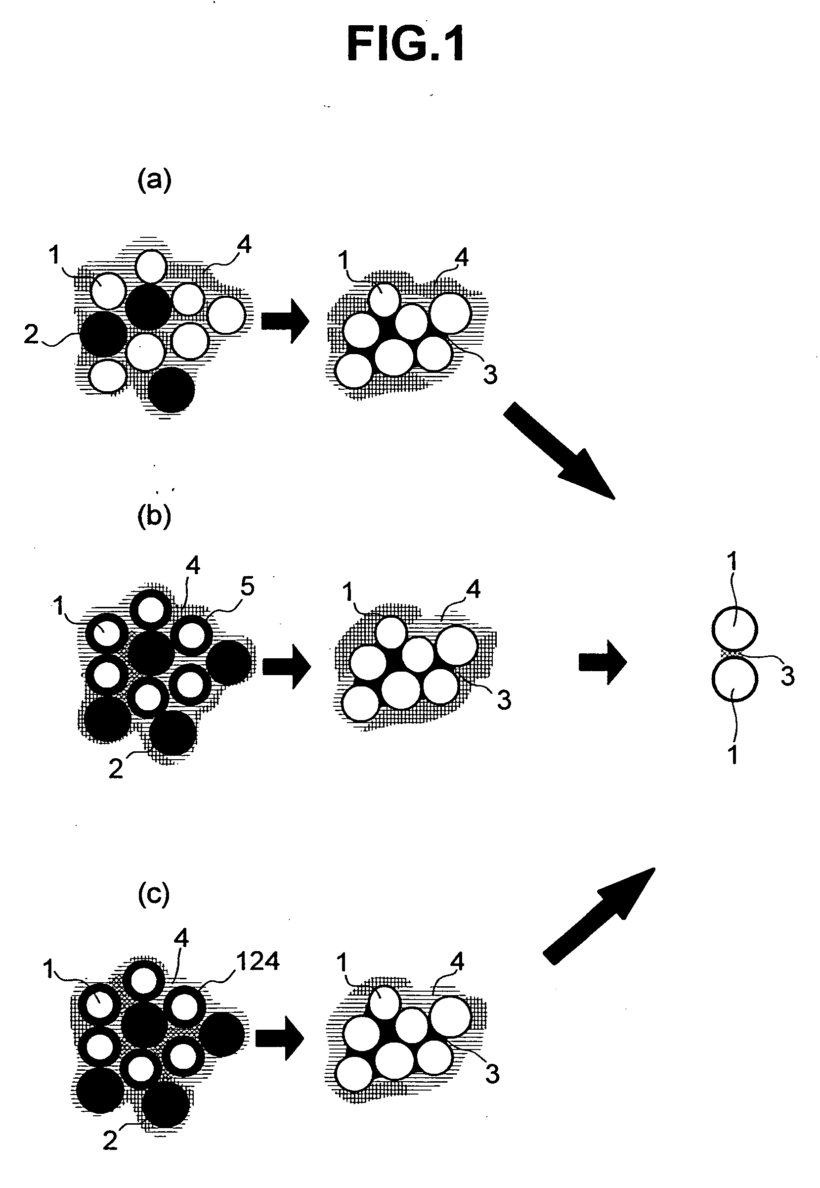
[0056]FIG. 1(a) to FIG. 1(c) show the concept of a bonding structure according to the invention. This drawing also shows the pre-soldering condition and the post-soldering condition. FIG. 1(a) shows an example that uses a paste in which Cu balls 1 with a particle size of about 30 μm (or balls of Ag, Au, Cu—Sn alloys or the like) and Sn-base solder balls 2 (melting point: 232 degrees centigrade) with a particle size of about 30 μm are appropriately dispersed in small quantities via a flux 4. When this paste is subjected to reflow at a temperature of not less than 250 degrees centigrade, Sn-base solder balls 2 melt, a molten Sn 3 spreads such that molten Sn 3 wets Cu balls 1 and is distributed relatively uniformly between Cu balls 1. Thereafter, Cu balls 1 and molten Sn 3 react with each other so that Cu balls 1 are connected to each other with the aid of compounds of Cu and Sn (mainly Cu6Sn5). The particle sizes of Cu balls 1 and Sn-base solder balls 2 are not limited to the above-me...

embodiment 2

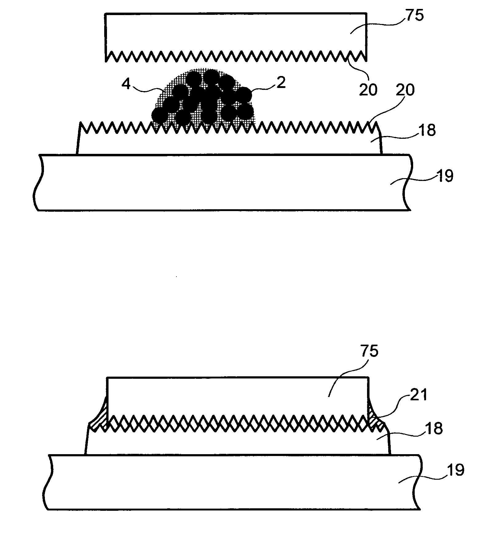
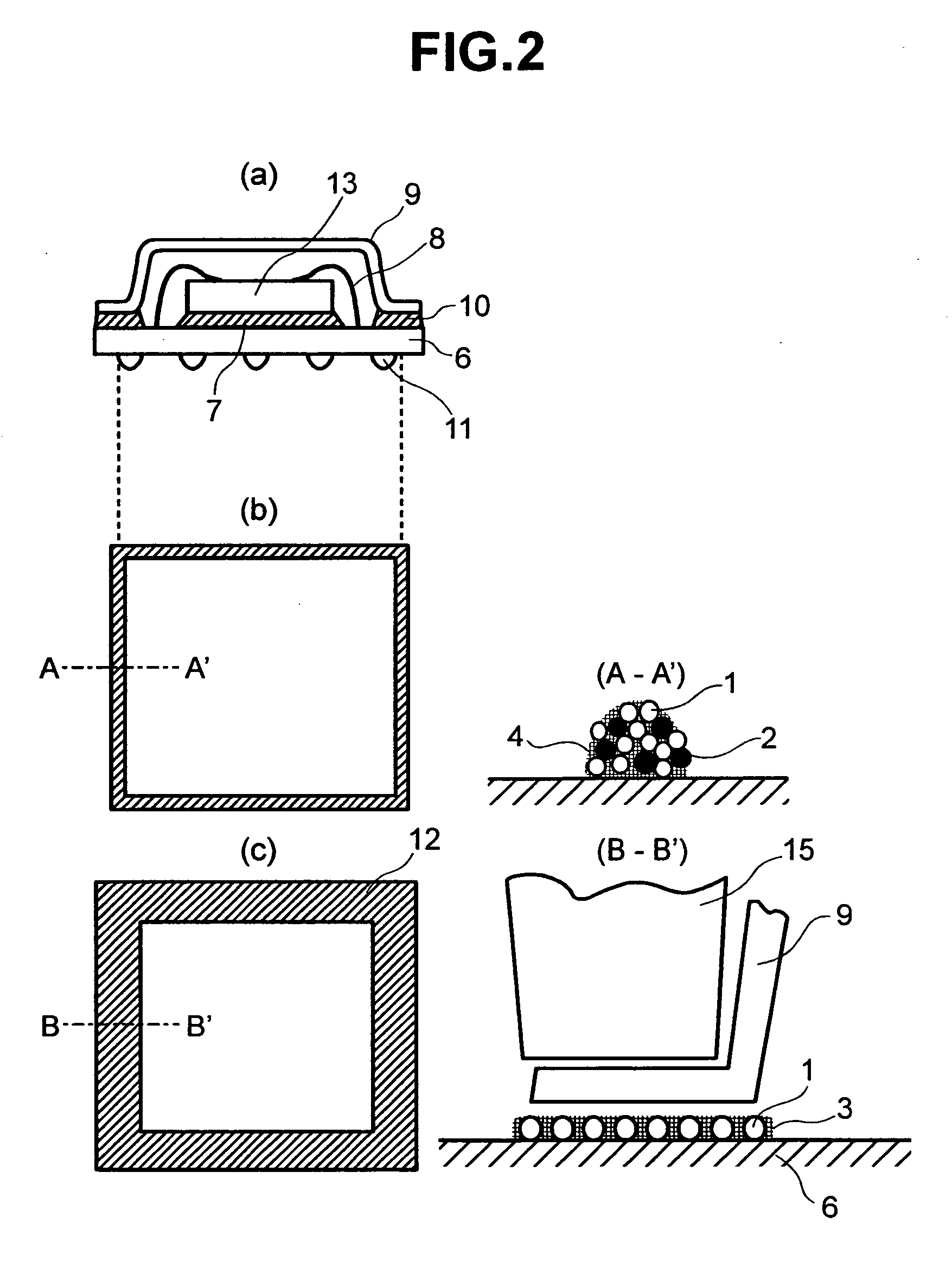
[0075] In FIG. 2(a), a semiconductor device 13 is bonded to a junction substrate 6 using an Au-20Sn solder 7 or the like. After wire bonding using gold wires 8 or the like, a peripheral portion of a cap 9, which is fabricated by applying a Ni—Au plating to an Al plate, a Fe—Ni plate or the like is bonded to junction substrate 6 by reflow through a solder paste 10 of the above-mentioned non-cleaning type. In this embodiment, when the insulating characteristic is regarded as important, it is desirable to perform bonding in a nitrogen atmosphere using a solder with a flux not containing chlorine. However, when wettability cannot be ensured, encapsulation with a weak-activity rosin of the RMA type may be performed. It is not necessary to ensure the complete encapsulation or the sealing of semiconductor device 13. That is, provided that the flux has sufficient insulating characteristics, even when semiconductor device 13 is held in the presence of the flux for a long time, the semiconduc...

embodiment 3

[0081] The paste according to the invention can be also used in die bonding 7 shown in FIG. 2(a). After bonding semiconductor device 13 using the paste according to the invention, cleaning and wire bonding are performed. In the prior art, die bonding uses Au-20Sn bonding. However, in view of reliability of the Au-20Sn solder, use of Au-20Sn solder has been limited to die mounting of small chips. Further, when die bonding is performed using a paste made of a Pb-base solder, a Pb-10Sn solder and the like have been used. The bonding according to the invention is also applicable to chips having a somewhat larger area. The larger the thickness of the bonding portion, the more service life is prolonged and reliability is increased. According to the invention, it is possible to increase this thickness by using high-melting-point balls each having a larger size. When decreasing the thickness, a smaller size of particles (balls) is used. In some bonding methods, it is also possible to form a...


PUM

PropertyMeasurementUnit
diameteraaaaaaaaaa
thicknessaaaaaaaaaa
thicknessaaaaaaaaaa

Abstract

In an electronic device which realizes high-temperature-side solder bonding in temperature-hierarchical bonding, a bonding portion between a semiconductor device and a substrate is formed of metal balls made of Cu, or the like, and compounds formed of metal balls and Sn, and the metal balls are bonded together by the compounds.

Description

CROSS-REFERENCE TO RELATED APPLICATION(S) [0001] This is a continuation of U.S. application Ser. No. 10 / 384,308, filed Mar. 7, 2003, and entitled “Electronic Device,” which application claimed priority from Japan Patent Application No. 2002-064250, filed Mar. 8, 2002.BACKGROUND OF THE INVENTION [0002] 1. Field of the Invention [0003] The present invention relates to an electronic device that uses a lead-free solder (solder that contains at most a trace amount of lead) and, more particularly to an electronic device fabricated by solder bonding using a temperature hierarchy that is effective in mounting a module formed of the electronic device or the like. [0004] 2. Description of Related Art [0005] In bonding using Sn—Pb-base solders, temperature-hierarchical bonding has been used. In this bonding technique, parts are soldered first at a temperature between 330 degrees centigrade and 350 degrees centigrade using solder for high-temperature soldering such as Pb-rich Pb-5 mass % Sn sol...

Claims


Application Information

Patent Timeline
Patent Type & Authority Applications(United States)
IPC IPC(8): H01L23/48B23K1/00B23K3/06B23K35/02B23K35/26B23K101/42C22C5/02C22C13/00H01L23/14H05K1/14H05K3/34
CPCB23K35/0244B23K35/262H01L2224/1134H01L2224/13144H01L2224/13147H01L2224/16H01L2224/48247H01L2224/49171H01L2924/01012H01L2924/01046H01L2924/01078H01L2924/01079H01L2924/09701H01L2924/13091H01L2924/14H01L2924/15153H01L2924/1517H01L2924/15311H01L2924/16152H01L2924/19041H05K1/141H05K3/3463H05K3/3484H05K2201/0215H05K2201/0218H05K2201/045H05K2201/10636H01L2224/48091H01L2924/00013H01L2924/01087H01L2924/01322H01L2224/32225H01L2224/32245H01L2224/48227H01L2224/48472H01L2224/73204H01L2224/73265H01L2224/45124H01L2224/45144H01L2924/19105H01L2924/01327H01L2924/10253H01L2224/16235H01L2924/00014H01L2224/13099H01L2924/00H01L2924/00012H01L2924/181H01L24/73H01L2224/05573H01L2224/05568H01L2224/05166H01L2224/05169H01L2224/05144H01L2224/0508H01L2224/05611H01L2224/03828H01L2224/11334H01L24/11H01L24/13H01L2224/11472H01L2224/13023H01L2224/13018H01L2224/13582H01L2224/13644H01L2224/13655H01L2224/16227H01L2224/13118H01L2224/13155H01L2224/16058H01L24/03H01L24/05H01L2224/05548H01L2224/13024H05K3/3485Y02P70/50H01L2224/05639H01L2224/05644H01L2224/05655H01L2224/05669H01L2924/014H01L2924/013H01L2924/0105H01L2924/01013H01L2224/16225H01L21/60
Inventor SOGA, TASAOHATA, HANAENAKATSUKA, TETSUYANEGISHI, MIKIONAKAJIMA, HIROKAZUENDOH, TSUNEO
Owner HITACHI LTD
Why Eureka
Try Eureka