

Method of pulsing vapor precursors in an ALD reactor
a gas phase deposition and precursor technology, applied in the direction of crystal growth process, polycrystalline material growth, chemically reactive gas production, etc., can solve the problems of insufficient film quality and thickness control, insufficient for many present-day microelectronic applications, and slow process of ald method, etc., to achieve short precursor pulses, improve pulse separation, and accelerate film growth
- Summary
- Abstract
- Description
- Claims
- Application Information
AI Technical Summary
Benefits of technology
Problems solved by technology
Method used
Image

Examples
Embodiment Construction
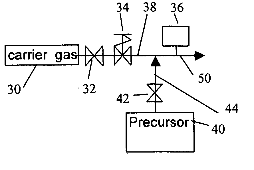
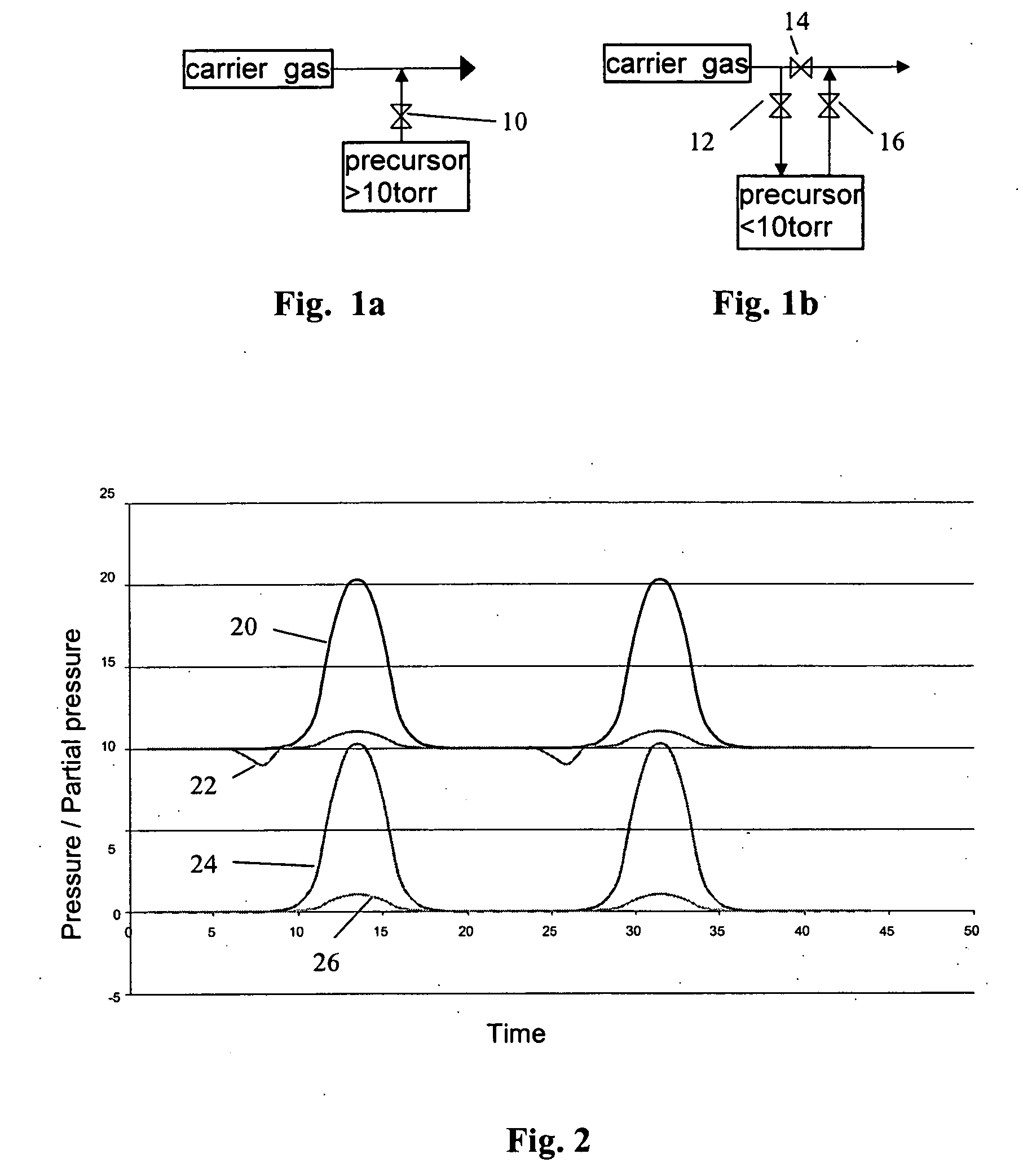
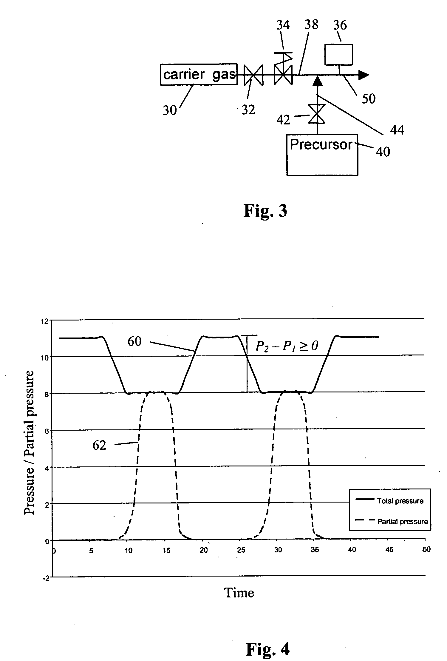
[0039] In the context of the description herein, “an ALD type process” generally refers to a process for producing thin films over a substrate, in which a solid thin film is formed molecular layer by molecular layer due to self-saturating chemical reactions on heated surfaces. In the process, gaseous reactants, i.e. precursors, are conducted into a reaction space of an ALD type of a reactor and contacted with a substrate located in the chamber to provide a surface reaction. The pressure and the temperature of the reaction space, including the substrate, are adjusted to a range where physisorption (i.e. low temperature condensation of gases) and thermal decomposition of the precursors are avoided. Consequently, only up to one monolayer (i.e. an atomic layer or a molecular layer) of material is deposited at a time during each pulsing cycle. The actual growth rate of the thin film, which is typically presented as angstroms per pulsing cycle (A / pulsing cycle), depends, for example, on t...
PUM
| Property | Measurement | Unit |
|---|---|---|
| pressure | aaaaa | aaaaa |
| Reynolds number | aaaaa | aaaaa |
| temperatures | aaaaa | aaaaa |
Abstract
Description
Claims
Application Information