Method of forming copper interconnections and thin films using chemical vapor deposition with catalyst

a technology catalyst, which is applied in the direction of chemical vapor deposition coating, semiconductor/solid-state device details, coatings, etc., can solve the problems of aluminum alloys being weak, the failure mechanism known as electromigration problems, and the grain size of aluminum alloys becoming more serious concerns

Inactive Publication Date: 2004-04-13
ASM KOREA LTD
View PDF8 Cites 188 Cited by
  • Summary
  • Abstract
  • Description
  • Claims
  • Application Information

AI Technical Summary

Problems solved by technology

However, aluminum alloys are known to be weak under high electrical as well as thermal stresses, causing a failure mechanism know as electromigration problem primarily due to the grain size.
Furthermore, as the device designrule becomes tighter, the grain size of aluminum alloys becomes more serious concern because of the aforementioned electromigration-related problems.
On the other hand, copper is significantly harder than aluminum, thereby it is difficult to etch compared to aluminum alloys, for which "deposit-and-then-etch" process can be readily applied.
However, this process does not conform very well and also is not compatible well with the conventional semiconductor processing steps.
Also, this process is rather complex and needs to be developed further in order to achieve high yield in a mass-production environment.
This is why the sputtering technique is not best suited yet for submicron class of semiconductor device manufacturing.
It has been reported, however, that when copper material is deposited by means of a CVD at about 200.degree. C. of the substrate temperature, not only the film growth rate decreases below 50 nm / minute, which is considered as a slow rate, but also the film surface becomes bumpy, because the thin film after its nucleation starts growing like islands at the beginning of the growth.
This method allows copper material deep into trenches and holes, thereby the deep trenches and holes can be filled with copper, while the conventional method such as sputtering technique would not allow such deep penetrations.

Method used


Image

  • Method of forming copper interconnections and thin films using chemical vapor deposition with catalyst
  • Method of forming copper interconnections and thin films using chemical vapor deposition with catalyst
  • Method of forming copper interconnections and thin films using chemical vapor deposition with catalyst

Examples


embodiment 1

Preferred Embodiment 1

A method of forming interconnecting conductors such as trenches, via holes, contacts using copper material by means of a copper chemical vapor deposition(CVD) process using catalyst is disclosed and described below in detail.

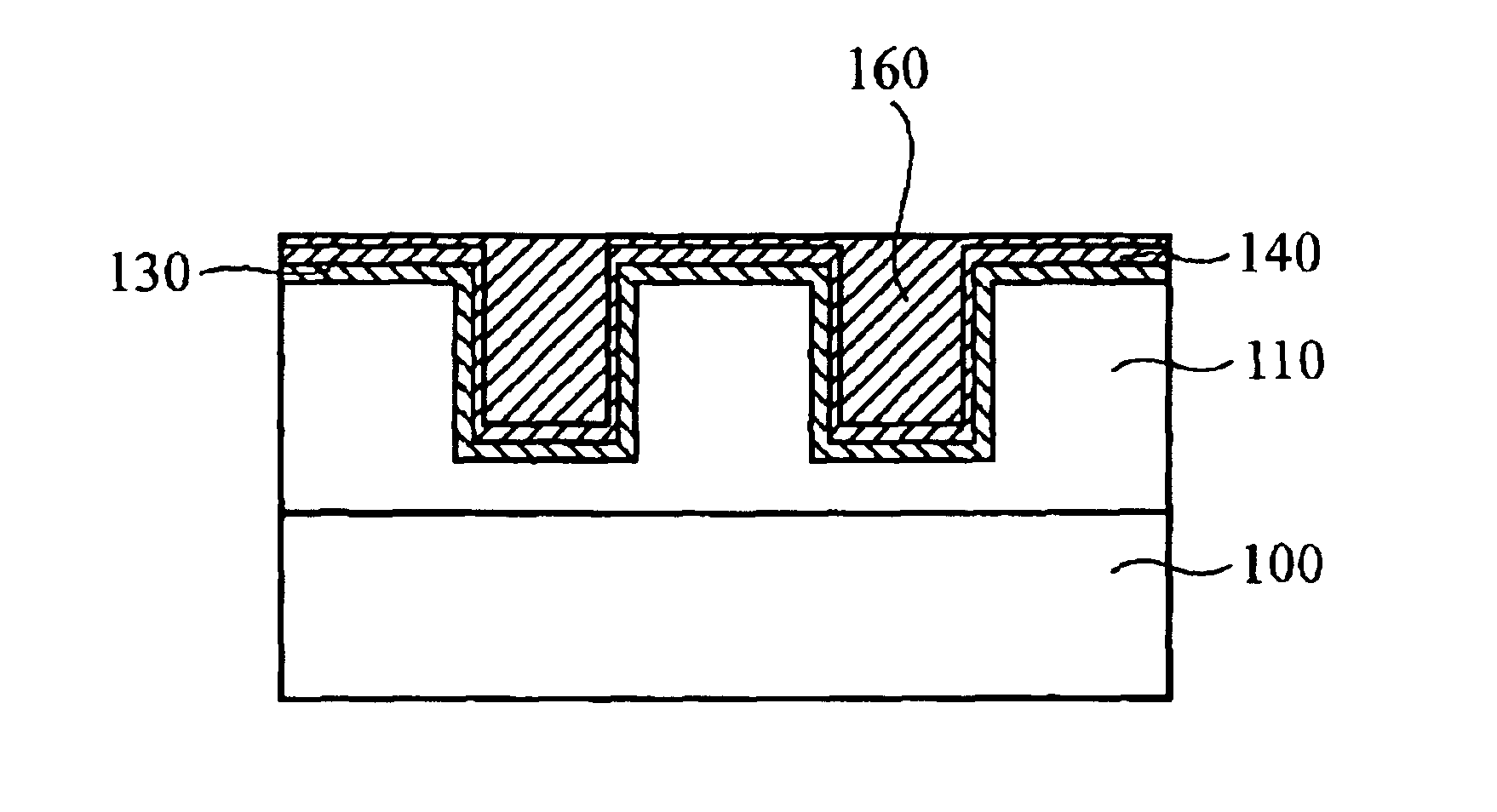
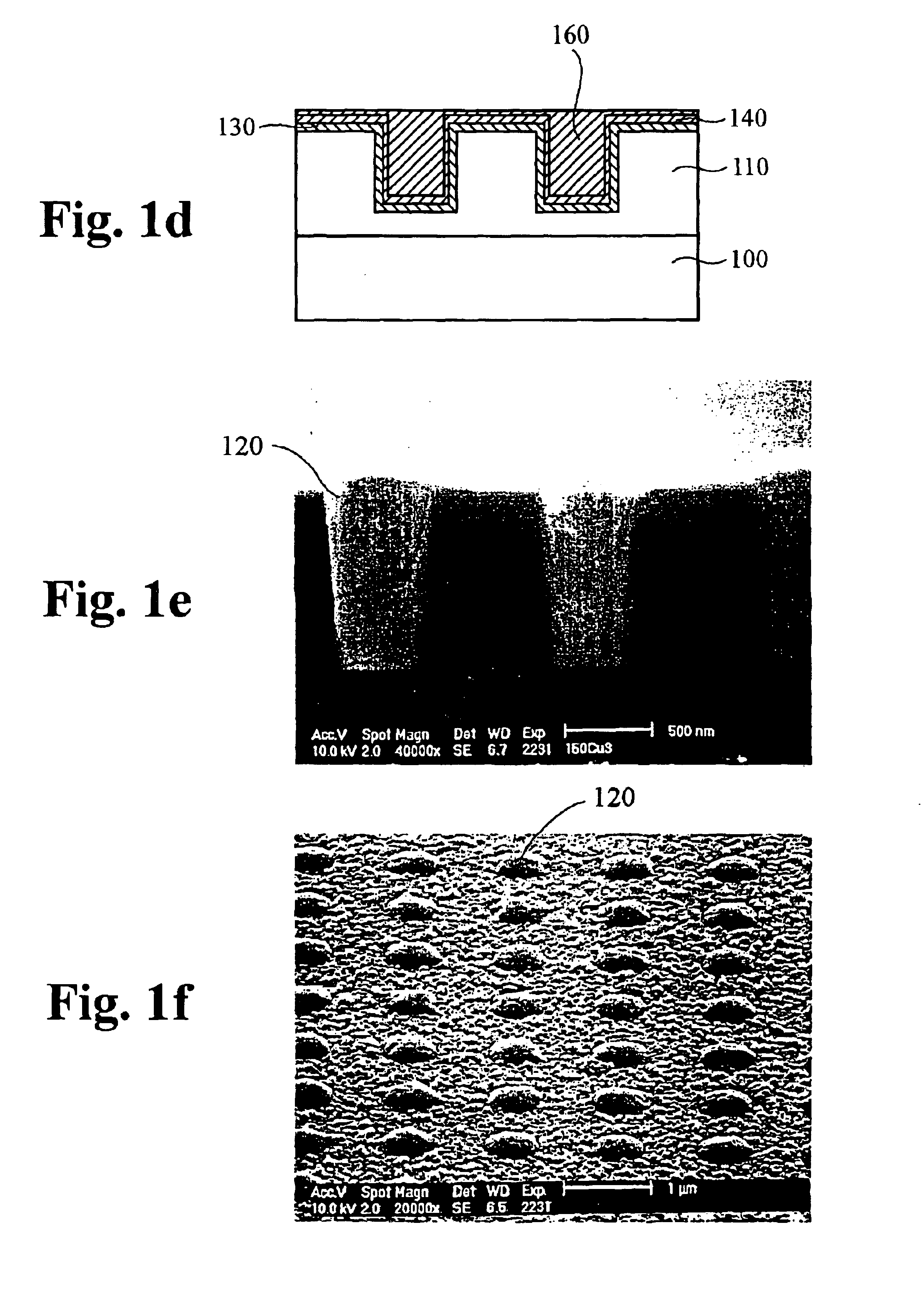
First step is preparation of samples. FIG. 1a shows a damascene structure by etching a hole 120 in an insulating layer 110 or the silicon substrate 100. This is a typical damascene structure. The top opening of a hole 120 is 500 nm in width and the aspect ratio is 2:1, (therefore, the depth of the hole 120 is 1000 nm). Referring to FIG. 1b, all surfaces including the hole 120 are covered with tantalum nitride(TaN) film 130 by means of sputtering. This tantalum nitride film acts as a barrier layer that prevents the conducting material 140 from penetrating into the insulating layer 110 during deposition process, where such penetration would, otherwise, alter the basic integrity of the conductor-insulator relationship, thereby defeating the pu...

embodiment 2

Preferred Embodiment 2

Interconnecting conductors imbedded into silicon substrates have many different shapes and sizes. The interconnecting conductors for power and signal applications are generally larger. However, as described in Preferred Embodiment 1 above, the copper fill method based on a copper CVD using catalyst according to the present invention is not well suited for filling a large area where the aspect ratio is very small such as a pad for input / output(I / O) signal and power lines.

Since damascene structures must be used in conjunction with copper deposition method according to the present invention because of the difficulty in etching copper materials unlike other "soft" metals such as aluminum alloys, a large trench with very small aspect ratio must be formed in order to use the copper fill method in accordance with the present invention.

Referring to FIG. 1i, a large trench 192 is formed in an insulating layer 190. However, a copper fill method in accordance with the pre...

embodiment 3

Preferred Embodiment 3

As afore-described in Preferred Embodiment 1, a silicon substrate sample with a barrier layer 230 and a seed layer 240 inside a trench 220 as well as on the top surface referring to FIG. 2a is prepared. In general, a sputtering method is used in forming barrier layer 230 as well as a seed layer 240. However, when the top opening of trenches and via holes are narrow, a CVD method may be used for forming a barrier layer 230 using TaN, or TiN and also a copper CVD method using ethyl-iodide as catalyst may be used for forming a seed layers 240. The copper source material (hfac)Cu(vtms) is again used here the same way as in Preferred Embodiment 1.

The catalyst ethyl-iodide is also applied as shown in FIG. 1c to form an additional copper layer 260 by means of a copper CVD using catalyst, whereby the second copper layer 260 is made thick enough (no more than 100 nm) to be used as an electrode for electroplating on top of the copper layer 260. Completely-filled copper l...


PUM

PropertyMeasurementUnit
depthaaaaaaaaaa
widthaaaaaaaaaa
aspect ratioaaaaaaaaaa

Abstract

A method of forming copper conductors for interconnecting active and passive elements as well as signal and power lines for circuits and devices on silicon wafers is disclosed. The method disclosed herein involves with using catalysts in conjunction with a chemical vapor deposition(CVD) process with typically using copper as a source material for forming interconnecting conductors. Interconnecting method for filling trenches, via holes, contacts, large trenches and holes for power devices and lines as well as for forming large passive elements is also disclosed. Disclosed herein are also a method of filling narrow and deep trenches and small in diameter and deep holes, and a method of forming very thin film on the flat top surface so that an etchback process, such as wet or dry etchback as well as plasma etchback processes, can be used for removing a thin film in preparation for subsequent processing steps, thereby rather expensive chemical mechanical polishing(CMP) process need not be used.

Description

1. Field of the InventionThis invention relates to the methods of forming copper-based interconnections such as trenches, via holes, contacts and thin films in the submicron class of semiconductor technology areas by means of chemical vapor deposition(CVD) method using catalyst.2. Description of the Related ArtInterconnecting active and passive elements as well as providing signal and power lines have been playing a vital role in the semiconductor-related product manufacturing processes.Most widely used method is to use aluminum-based metals by means of deposition, etching, etc. because aluminum alloys are relatively easy to handle for processing, easy to obtain and inexpensive. However, aluminum alloys are known to be weak under high electrical as well as thermal stresses, causing a failure mechanism know as electromigration problem primarily due to the grain size.Furthermore, as the device designrule becomes tighter, the grain size of aluminum alloys becomes more serious concern b...

Claims


Application Information

Patent Timeline
Patent Type & Authority Patents(United States)
IPC IPC(8): C23C16/02C23C16/04C23C16/44H01L21/70H01L23/532H01L23/485H01L21/768H01L23/52H01L23/48C23C16/18H01L21/28H01L21/285H01L21/3205
CPCC23C16/02C23C16/045C23C16/44H01L21/76802H01L21/7684H01L21/76873H01L21/76877H01L21/76885H01L23/53238H01L24/02H01L2924/01003H01L2924/01004H01L2924/01005H01L2924/01006H01L2924/01013H01L2924/01014H01L2924/01018H01L2924/01022H01L2924/01029H01L2924/0105H01L2924/01057H01L2924/01073H01L2924/01079H01L2924/04941H01L2924/04953H01L2924/01033H01L2924/351H01L2924/00H01L21/28
Inventor KOH, WON YONGPARK, HYUNG SANGLEE, JI HWA
Owner ASM KOREA LTD
Why Eureka
Try Eureka