Scanning transmission electron microscope and scanning transmission electron microscopy

a transmission electron microscope and scanning technology, applied in the field of scanning transmission electron microscopes, can solve the problems of unnecessary complicated and troublesome adjustment tasks, complicated and troublesome device adjustments, etc., and achieve the effects of improving the usability of the device, enlarge the field of view of the stem image, and improving the accuracy of correction accuracy

Active Publication Date: 2006-07-13
HITACHI HIGH-TECH CORP
View PDF1 Cites 15 Cited by
  • Summary
  • Abstract
  • Description
  • Claims
  • Application Information

AI Technical Summary

Benefits of technology

[0013] The enhancement in the correction accuracy makes it possible to enlarge the field-of-view of the STEM image. This tremendously improves the usability of the device. Also, it becomes possible to make smaller the hole diameter of the angle selection aperture 13. This also allows an enhancement in the selection accuracy of the transmitted electron beam.

Problems solved by technology

In the conventional control system, however, implementation of an enhancement in the correction accuracy has required a complicated and troublesome device adjustment.
This makes the complicated and troublesome adjustment task unnecessary.

Method used


Image

  • Scanning transmission electron microscope and scanning transmission electron microscopy
  • Scanning transmission electron microscope and scanning transmission electron microscopy
  • Scanning transmission electron microscope and scanning transmission electron microscopy

Examples


embodiment 1

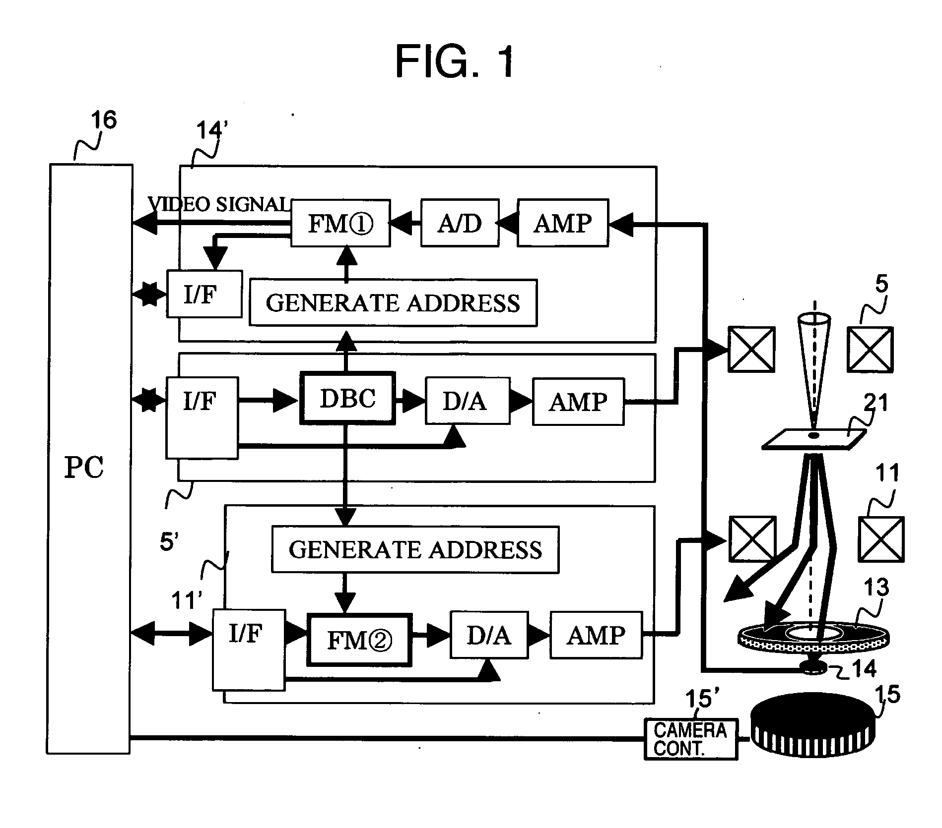
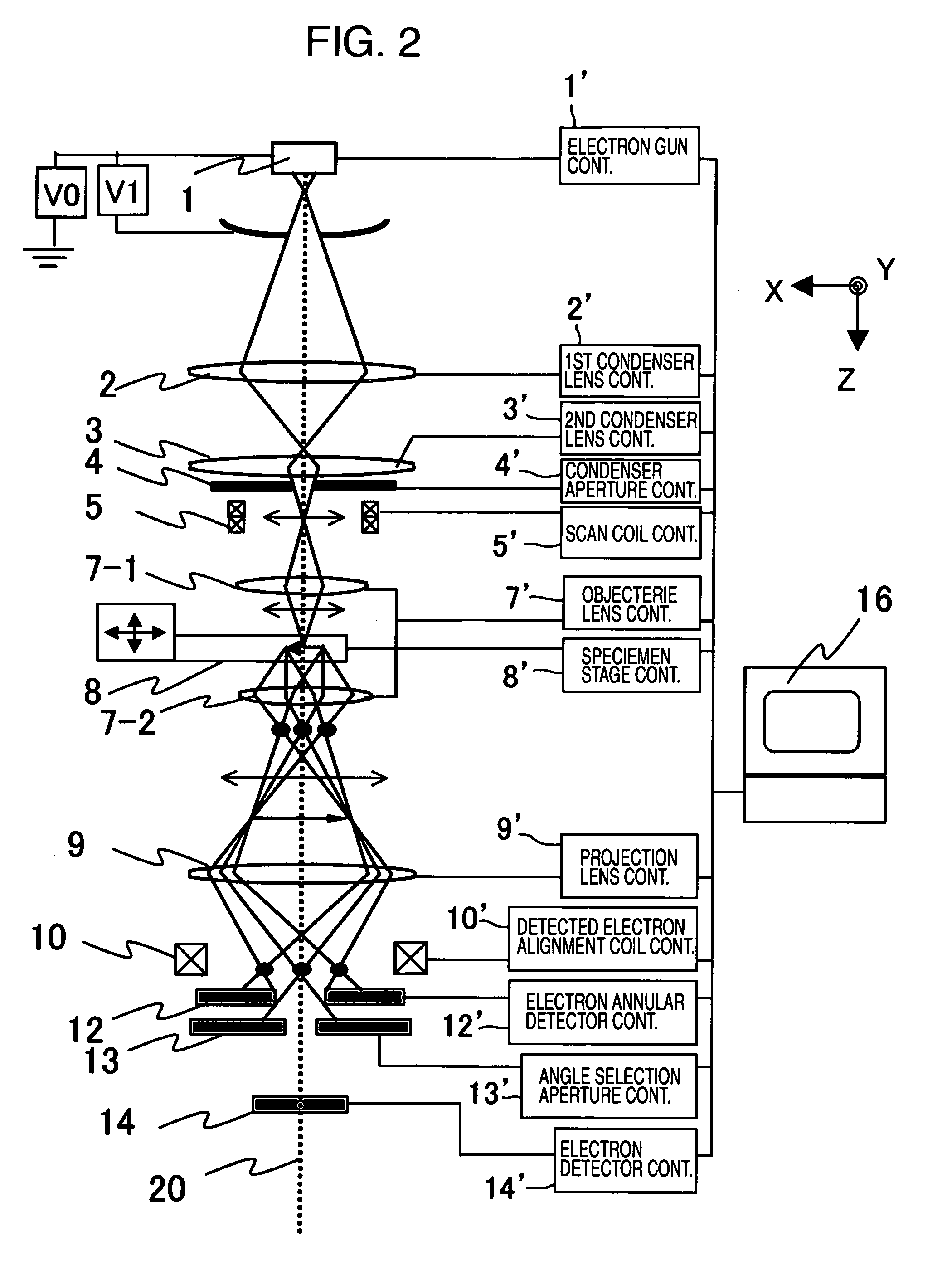
[0036] Hereinafter, the explanation will be given below concerning a first embodiment. FIG. 3 illustrates the basic configuration diagram of the STEM used in the present embodiment. The direction parallel to an optical axis 20 of the housing is defined as the Z direction, and the plane perpendicular to the optical axis is defined as the XY plane. The present STEM includes the following configuration components: An electron gun 1 for emitting a primary electron beam, a first condenser lens 2 and a second condenser lens 3 for forming in shape the primary electron beam emitted from the electron gun 1, a condenser aperture 4 for restricting an aperture angle of the primary electron beam, a scanning coil 5 for allowing the primary electron beam to be scanned on a specimen, an objective lens 7 for allowing focal point of the primary electron beam to be achieved on the specimen, a specimen stage 8 for holding the specimen 21, a secondary-electron detector 6 for detecting secondary electron...

embodiment 2

[0060] In the first embodiment, as the de-scanning coil 11, the one-stage deflection coil has been used which is set up between the projection lens 9 and the electron detector 14. It is also possible, however, to carry out the de-scanning by using some other coil. For example, as illustrated in FIG. 13, carrying out the de-scanning by using a two-stage deflection coil is also allowable. The two-stage deflection exhibits a disadvantage that the deflection quantity becomes smaller than that of the one-stage deflection. However, the two-stage deflection exhibits an advantage that it becomes possible to adjust both of the angle and the position of the electron beam.

[0061] Also, in order to clarify the functions of the respective coils, the detected-electron alignment coil 10 and the de-scanning coil 11 have been described in the separate manner. It is also possible, however, to implement these functions by using a single coil. Namely, if it is wished to simplify the coil control mechan...

embodiment 3

[0062]FIG. 16 illustrates a basic configuration diagram of the STEM-EELS used in the present embodiment. The EELS is installed on the lower portion of the STEM. In order to allow the transmitted electron beam to be detected by the EELS, as is the case with the angle selection aperture 13 and the electron detector 14, the electron detection camera 15 is also formed into a movable-type mechanism. The EELS includes a quadrupole lens 31, an accelerator 32, an electron spectrometer 33, a quadrupole magnifying lens 34, an energy slit 35, a mapping-use electron detector 36, a spectrum-use electron detector 37, and control units therefor.

[0063] Next, the explanation will be given below concerning processing steps for acquiring an EELS image by using the device illustrated in FIG. 16. First of all, the STEM image is acquired in accordance with the processing steps illustrated in the first embodiment. Moreover, a transmitted electron beam to which an energy spectroscopy is to be applied is s...


PUM


Abstract

A scanning transmission electron microscope which enhances correction accuracy of a de-scanning coil for canceling a transmitted-electron-beam position change on an electron detector. Here, this transmitted-electron-beam position change appears in accompaniment with a primary-electron-beam position change on a specimen caused by a scanning coil. First, control over the scanning coil is digitized. Moreover, while being synchronized with a digital control signal resulting from this digitization, values in a de-scanning table registered in a FM (2) are outputted to the de-scanning coil. Here, the de-scanning table is created as follows: Diffraction images before and after activating the scanning coil and the de-scanning coil are photographed using a camera. Then, based on a result acquired by analyzing a resultant displacement quantity of the diffraction images by the image processing, the de-scanning table is created.

Description

INCORPORATION BY REFERENCE [0001] The present application claims priority from Japanese application JP 2005-004660 filed on Jan. 12, 2005, the content of which is hereby incorporated by reference into this application. BACKGROUND OF THE INVENTION [0002] The present invention relates to a scanning transmission electron microscope (: STEM). More concretely, it relates to a control device and method for controlling an electron beam which has passed through a specimen. [0003] The STEM is a device for visualizing specimen structure with a sub-nanometer high space resolution. A raster scanning of an electron beam which is converged down to a nanometer order is performed on a specimen whose film is thinned down to a few hundreds of nm. Moreover, a signal generated from an electron-beam irradiation area is detected, then being synchronized with the raster scanning. This synchronization allows the two-dimensional image to be formed. Examples of the signal generated from the electron-beam irr...

Claims


Application Information

Patent Timeline
Patent Type & Authority Applications(United States)
IPC IPC(8): G21K7/00
CPCH01J37/1474H01J37/2955H01J2237/1501H01J2237/221H01J2237/2802
Inventor TSUNETA, RURIKOKOGUCHI, MASANARIHASHIMOTO, TAKAHITONAKAMURA, KUNIYASU
Owner HITACHI HIGH-TECH CORP
Why Eureka
Try Eureka