Memory cell power switching circuit in semiconductor memory device and method for applying memory cell power voltage

a technology of memory cell and switching circuit, which is applied in the direction of digital storage, pipes, instruments, etc., can solve the problems of deteriorating prior art is not optimal for employment in several fields, and the current characteristic of memory devices may be deteriorated, so as to reduce standby current, shorten wake-up time, and suppress leakage current

Active Publication Date: 2006-07-13
SAMSUNG ELECTRONICS CO LTD
View PDF6 Cites 18 Cited by
  • Summary
  • Abstract
  • Description
  • Claims
  • Application Information

AI Technical Summary

Benefits of technology

[0014] Various aspects of the present invention provide a technique and a semiconductor memory device that reduce standby current without degrading the operating characteristic of a device and that shorten the wake-up time so that a memory cell power voltage is rapidly recovered (from a lower, standby level) to a stable level of a (higher) operating voltage, without degrading the operating characteristic when a standby mode is switched to an operation mode.
[0032] According to the structure of the circuit, it is possible to suppress leakage current in a standby operation and shorten a wake-up time when the standby mode is switched to an operation mode. It is also possible to reduce standby current without degradation of an operation characteristic of a device by applying a standby voltage as a cell power voltage only in a deep standby mode in which a standby mode lasts for a relatively long time.

Problems solved by technology

In such a technique, the current characteristic of a memory device may be deteriorated due to very great load capacitance when the standby state is switched to the operating state.
Thus, while the above-described prior art can reduce the standby current there may be degradation of a device current characteristic, and the prior art is not optimal for employment in several fields.
However, if the memory cell power voltage applied to the load transistors T3 and T4 is changed from a (lower) standby voltage to a (higher) operating voltage immediately after the standby mode is changed to the operation mode, load capacitance becomes very large due to a change in a cell power load.
This increases the cell wake-up time and degrades an operating characteristic of the semiconductor memory device.
Further, if the device enters a standby mode (when a standby voltage lower than the operation voltage is applied) e.g., whenever a memory cell block including memory cells is not selected during a relatively short period of time, stability of the operation is not guaranteed due to too frequent wake-ups.

Method used


Image

  • Memory cell power switching circuit in semiconductor memory device and method for applying memory cell power voltage
  • Memory cell power switching circuit in semiconductor memory device and method for applying memory cell power voltage
  • Memory cell power switching circuit in semiconductor memory device and method for applying memory cell power voltage

Examples


first embodiment

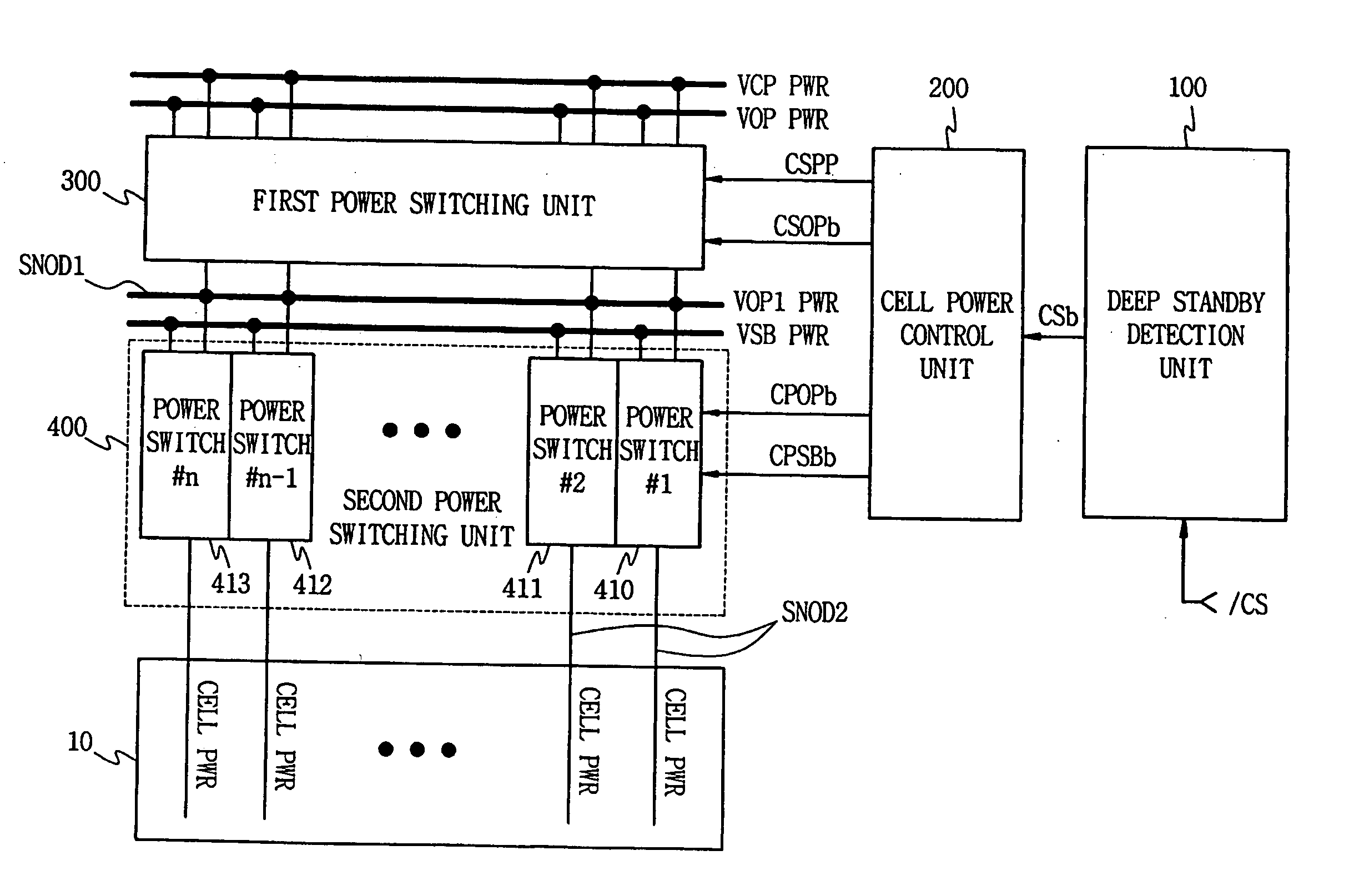
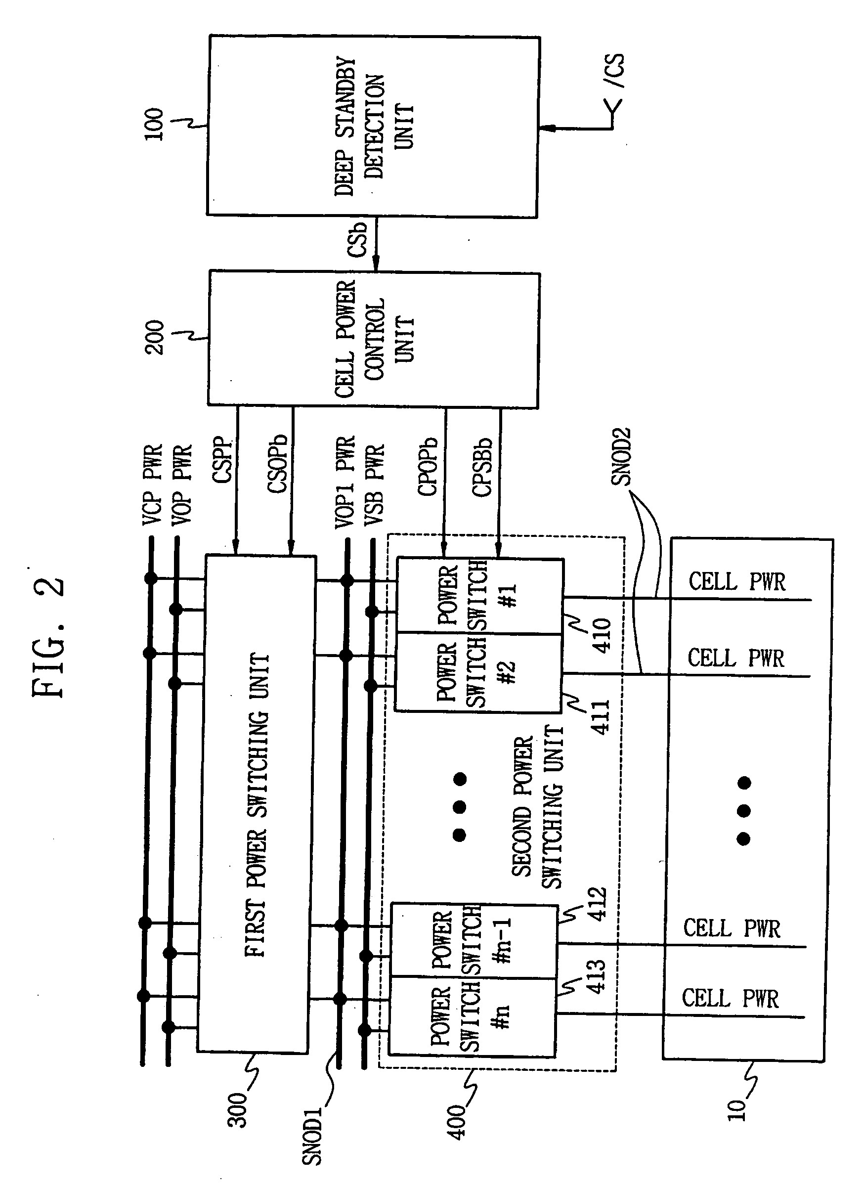
[0045]FIG. 2 is a block diagram of a memory cell power switching circuit according to the present invention. In FIG. 2, a dual power mode switching structure used for controlling memory cell power in a memory cell is schematically shown. The memory cell power switching circuit of FIG. 2 can be formed on a semiconductor memory device chip.

[0046] Referring to FIG. 2, the circuit includes a deep standby detection unit 100, a cell power control unit 200, a first power switching unit 300, a second power switching unit 400, and a memory cell array 10.

[0047] The first power switching unit 300 selectively outputs one of an operation voltage VOP PWR or a high power supply voltage VCP PWR (higher than the operation voltage VOP PWR) to a first switching output stage SNOD1 in response to first switch control signals CSPP and CSOPb, respectively, applied by the cell power control unit 200.

[0048] The second power switching unit 400 includes a plurality of power switches 410 to 413 for selective...

second embodiment

[0058]FIG. 4 is a block diagram of a memory cell power switching circuit according to the present invention. Referring to FIG. 4, a memory cell power switching block 500 is a dual mode power switching structure, and includes a memory cell power control unit 200, a first power switching unit 300, and a second power switching unit 400), is operatively integrated with a memory cell array 10 (similarly as shown in FIG. 2). Further, in FIG. 4, the cell power switching circuit comprises a dual mode power switching structure (each comprised of a memory cell power switching block 500) connected at each end of the memory cell array 10 so that the cell power applying operation as described with reference to FIG. 3 is performed (mirrored) at both ends of the memory cell array 10, thereby resulting in a shorter wake-up time.

[0059] Similarly, FIG. 5 shows a block diagram of a cell power switching circuit according to a third exemplary embodiment of the present invention. In the case of FIG. 5, t...


PUM


Abstract

A power (voltage) switching circuit in a semiconductor memory device, capable of reducing leakage current in a standby mode of operation and shortening the wake-up time when a standby mode is switched to an operation mode. The power (voltage) switching circuit comprises a first power switch, a second power switch, and a third power switch operatively connected to at least one bitline in a memory cell array, configured to selectively output, as a cell power voltage, a dynamically selected one of a first power supply voltage, a second power supply voltage, and a third power supply voltage, respectively in response to a first, second or third applied switch control signals. The second power supply voltage being higher than the first power supply voltage and, the third power supply voltage being lower than the first power supply voltage. A cell power control unit controls states of the first, second and third switch control signals so that the cell power voltage is applied as the third (lowest) power supply voltage in a standby state and that when the standby state is switched to an operating state the cell power voltage is supplied as the second (highest) power supply voltage during a predefined period of time and then as the first power supply voltage.

Description

CROSS-REFERENCE TO RELATED APPLICATION [0001] This application claims the priority, under 35 U.S.C. § 119, of Korean Patent Application No. 10-2005-0003109, filed Jan. 13, 2005, the contents of which is hereby incorporated herein by reference in its entirety. BACKGROUND OF THE INVENTION [0002] 1. Technical Field [0003] The present invention relates to memory cell power supply in a semiconductor memory, and more particularly, to a memory cell power switching circuit in a volatile semiconductor memory device, such as a static random access memory (SRAM), and a method for applying a memory cell power voltage. [0004] 2. Discussion of Related Art [0005] As processor based systems such as personal computers and electronic communication devices achieve higher performance, greater speed and higher—integration, the performance of volatile semiconductor memory devices such as static random access memories (SRAMs) has correspondingly been increased. In a semiconductor memory device used in mob...

Claims


Application Information

Patent Timeline
Patent Type & Authority Applications(United States)
IPC IPC(8): G11C11/00
CPCG11C5/147G11C11/417F16L9/12
Inventor PARK, CHUL-SUNG
Owner SAMSUNG ELECTRONICS CO LTD
Why Eureka
Try Eureka