Coated conductive particle coated conductive particle manufacturing method anisotropic conductive material and conductive connection structure

a technology of anisotropic conductive material and manufacturing method, which is applied in the direction of natural mineral layered products, cellulosic plastic layered products, transportation and packaging, etc., can solve the problems of defective conduction, short circuit and the like between adjacent electrodes, and difficulty in forming an insulating coating layer with a constant thickness, etc., to achieve superior connection reliability

Inactive Publication Date: 2006-07-13
SEKISUI CHEM CO LTD
View PDF5 Cites 66 Cited by
  • Summary
  • Abstract
  • Description
  • Claims
  • Application Information

AI Technical Summary

Benefits of technology

[0009] An objective of the present invention is to provide a coated conductive particle having superior connection reliability, a

Problems solved by technology

In order to ensure high connection reliability, it is necessary to increase the blended amount of conductive particles in an anisotropic conductive material, and in the case of a circuit board and the like having such fine wires, conduction or the like in a lateral direction may occur between adjacent conductive particles to cause problems of short circuit and the like between adjacent electrodes.
In these methods, however, it is difficult to form an insulating coating layer with a constant thickness, and in some cases, a plurality of conductive particles are simultaneously coated.
In the case where conductive connection is made by using coated conductive particles, if the thickness of the insulating coating layer is not uniform, a pressure is not transmitted uniformly upon fixing the layer between electrodes even when the particle size of the conductive particles is precisely controlled, with the result that a defective conduction may occur.
For example, in the case of the above-mentioned formation method of the insulating coat by the hybridization process, since insulating resin particles to form a coating layer are made to adhere to the surfaces of the conductive particles by a physical force in this method, it is not possible to form the coating layer on the surface of each of the conductive particles as a single layer, with the result that it becomes difficult to control the thickness of the insulating coating layer, and since the resin particles are fused and deformed due to heat and impact caused by the heating process and frictional heat, it is difficult to prepare an uniform coating layer.
Moreover, since the contact area between the insulating resin particles and the metal surface becomes greater, it is difficult to remove the insulating coating layer in the case where a device to which it is difficult to apply heat and pressure, such as a liquid crystal element, is used, with the result that a defective conduction may occur.
However, in the coated conductiv

Method used


Image

  • Coated conductive particle coated conductive particle manufacturing method anisotropic conductive material and conductive connection structure
  • Coated conductive particle coated conductive particle manufacturing method anisotropic conductive material and conductive connection structure

Examples


example 1

[0101] Insulating particles [1] were dispersed in distilled water under irradiation with ultrasonic wave to obtain an aqueous dispersion solution having 10% by weight of insulating particles [1].

[0102] In 500 mL of distilled water were dispersed 10 g of metal surface particles [1], and to this was added 4 g of aqueous dispersion solution of insulating particles [1], and stirred at room temperature for 6 hours. After having been filtered through a mesh-filter of 3 μm, this was further washed with methanol, and dried to obtain coated conductive particles [1].

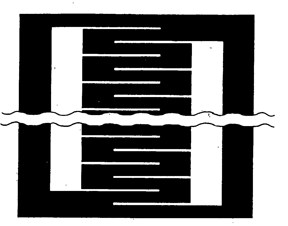
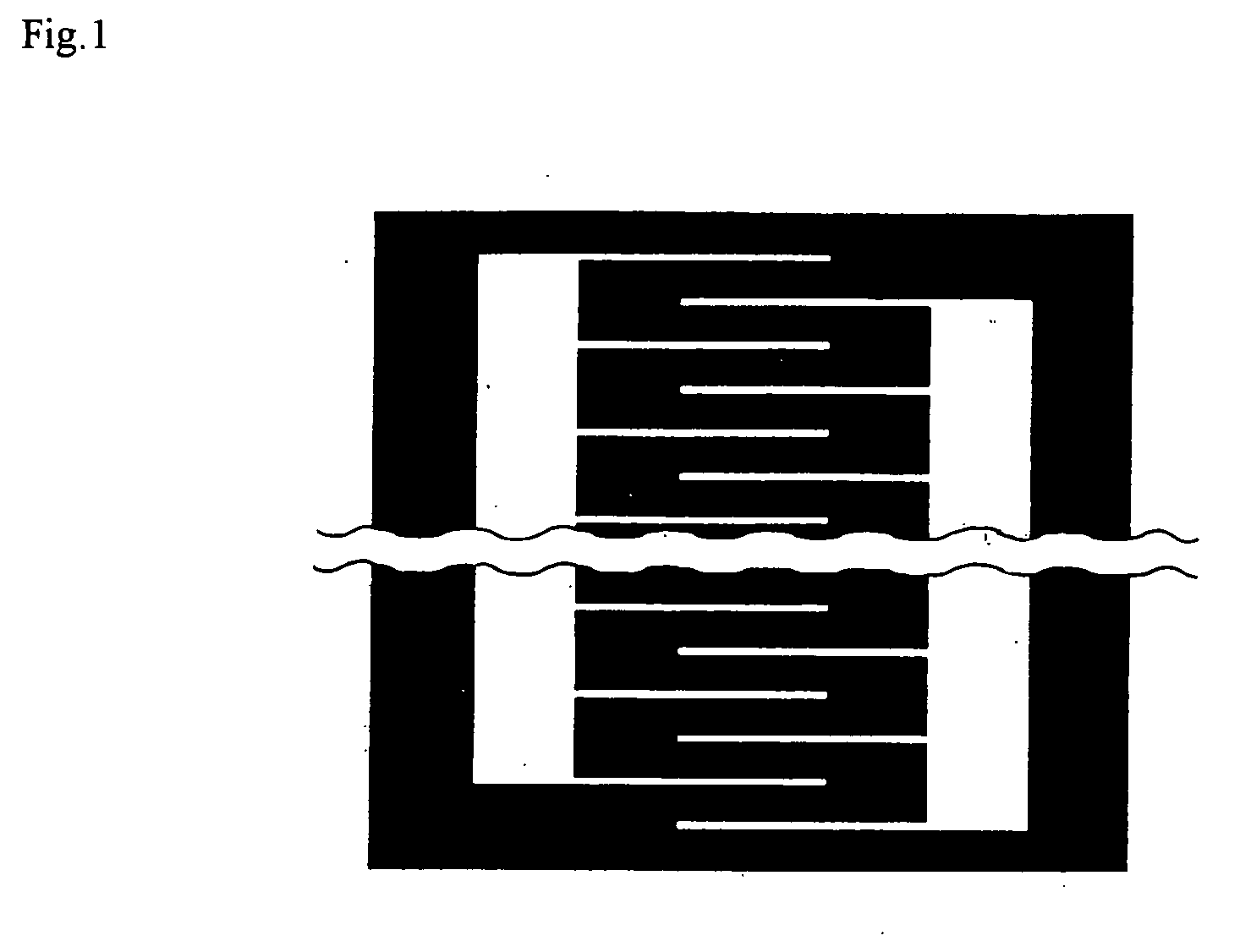
[0103] When each of coated conductive particles [1] was observed under a scanning electronic microscope (SEM), only one coating layer was formed on the surface of each of metal surface particles [1] by insulating particles [1]. When the coated area (that is, the projection area of the particle size of each insulating particle) of the insulating particles with respect to an area of 2.5 μm from the center of the coated conductive ...

example 2

[0106] Insulating particles [2] were dispersed in acetone under irradiation with ultrasonic wave to obtain an acetone dispersion solution having 10% by weight of insulating particles [2].

[0107] In 500 mL of acetone were dispersed metal surface particles [1], and to this was added 4 g of acetone dispersion solution of insulating particles [2], and stirred at room temperature for 12 hours. After having been filtered through a mesh-filter of 3 μm, this was further washed with methanol, and dried to obtain coated conductive particles [2].

[0108] In coated conductive particles [2], only one coating layer was formed on the surface of each of metal surface particles [1] by insulating particles [2]. When measured in the same method as example 1, the coating rate thereof was 70%, and the interface bonding area was 15% of the surface area of the insulating particle. Moreover, when the state thereof after having been thermocompression-bonded between silicon wafers was observed under an SEM in...

example 3

[0110] Insulating particles [3] were dispersed in toluene under irradiation with ultrasonic wave to obtain a toluene dispersion solution having 10% by weight of insulating particles [3].

[0111] In 500 mL of toluene were dispersed metal surface particles [2], and to this was added 4 g of the toluene dispersion solution of insulating particles [3], and stirred at room temperature for 4 hours. After having been filtered through a mesh-filter of 3 μm, this was further washed with acetone, and dried to obtain coated conductive particles [3].

[0112] In coated conductive particles [3], only one coating layer was formed on the surface of each of metal surface particles [2] by insulating particles [3]. When measured in the same method as example 1, the coating rate thereof was 40%, and the interface bonding area was 5% of the surface area of the insulating particle. Moreover, when the state thereof after having been thermocompression-bonded between silicon wafers was observed under an SEM in...


PUM

PropertyMeasurementUnit
Fractionaaaaaaaaaa
Fractionaaaaaaaaaa
Temperatureaaaaaaaaaa

Abstract

An objective of the invention is to provide a coated conductive particle having superior connection reliability, a method for manufacturing such coated conductive particle, an anisotropic conductive material and a conductive-connection structure. A coated conductive particle comprising a particle having a surface made of conductive metal and an insulating particles to coat the surface of the particle having the surface made of conductive metal there with, wherein the insulating particles are chemically bonded to the particle having the surface made of conductive metal via a functional group (A) having a bonding property to the conductive metal so that a single coating layer is formed.

Description

TECHNICAL FIELD [0001] The present invention relates to a coated conductive particle having superior connection reliability, a method for manufacturing such coated conductive particle, an anisotropic conductive material and a conductive-connection structure. BACKGROUND ART [0002] Particles, each having a metal surface, have been used as various resin fillers, modifying agents and the like, and in addition to these usages, those particles are mixed in a binder resin as conductive particles, and used as so-called anisotropic conductive materials that electrically connect miniature-size electrical parts such as semiconductor elements to circuit boards, or electrically connect circuit boards to each other, in electronic products such as liquid crystal displays, personal computers and portable communication devices. [0003] In recent years, along with the developments of miniature-size electronic apparatuses and electronic parts, wires on circuit boards and the like have become finer, and...

Claims


Application Information

Patent Timeline
IPC IPC(8): B32B5/16B22F1/102H01R13/03H01R13/24H05K3/32
CPCB22F1/0062B22F2998/00H05K3/323H05K2201/0212H05K2201/0221Y10T428/2991H05K2201/0233H05K2201/0224Y10T428/2998B22F1/025B22F1/102B22F1/17H01B1/20
Inventor WAKIYA, TAKESHIYONEDA, YOSHIKAZUUEBA, MASAKO
Owner SEKISUI CHEM CO LTD
Why Eureka
Try Eureka