Gap fill materials and bottom anti-reflective coatings comprising hyperbranched polymers

a polymer and filling technology, applied in the direction of photosensitive materials, instruments, photomechanical equipment, etc., can solve the problems of reducing the resolution of the photoresist, affecting the image quality of the processed photoresist, and reducing the adhesion of the active radiation back into the photoresist by the substrate, etc., to achieve superior coverage and low viscosity

Active Publication Date: 2006-07-13
BREWER SCI
View PDF7 Cites 24 Cited by
  • Summary
  • Abstract
  • Description
  • Claims
  • Application Information

AI Technical Summary

Benefits of technology

[0021] The method of applying the anti-reflective or fill compositions to a substrate having a contact or via hole simply comprises applying a quantity of a composition hereof to the substrate surfaces forming the hole by any conventional application met

Problems solved by technology

However, a frequent problem encountered by photoresists during the manufacturing of semiconductor devices is that activating radiation is reflected back into the photoresist by the substrate on which it is supported.
Such reflectivity tends to cause blurred patterns which degrade the resolution of the photoresist.
Degradation of the image in the processed photoresist is particularly problematic when the substrate is non-planar and/or highly reflective.
These inorganic films are conformal and difficult to remove after the photolithography step.
One major drawback of linear chain polymers, however, is that they undergo chain entanglements, leading

Method used


Image

  • Gap fill materials and bottom anti-reflective coatings comprising hyperbranched polymers
  • Gap fill materials and bottom anti-reflective coatings comprising hyperbranched polymers
  • Gap fill materials and bottom anti-reflective coatings comprising hyperbranched polymers

Examples


example 1

Formulation of Gap Fill Material for Exposure Wavelengths of Less Than 400 nm

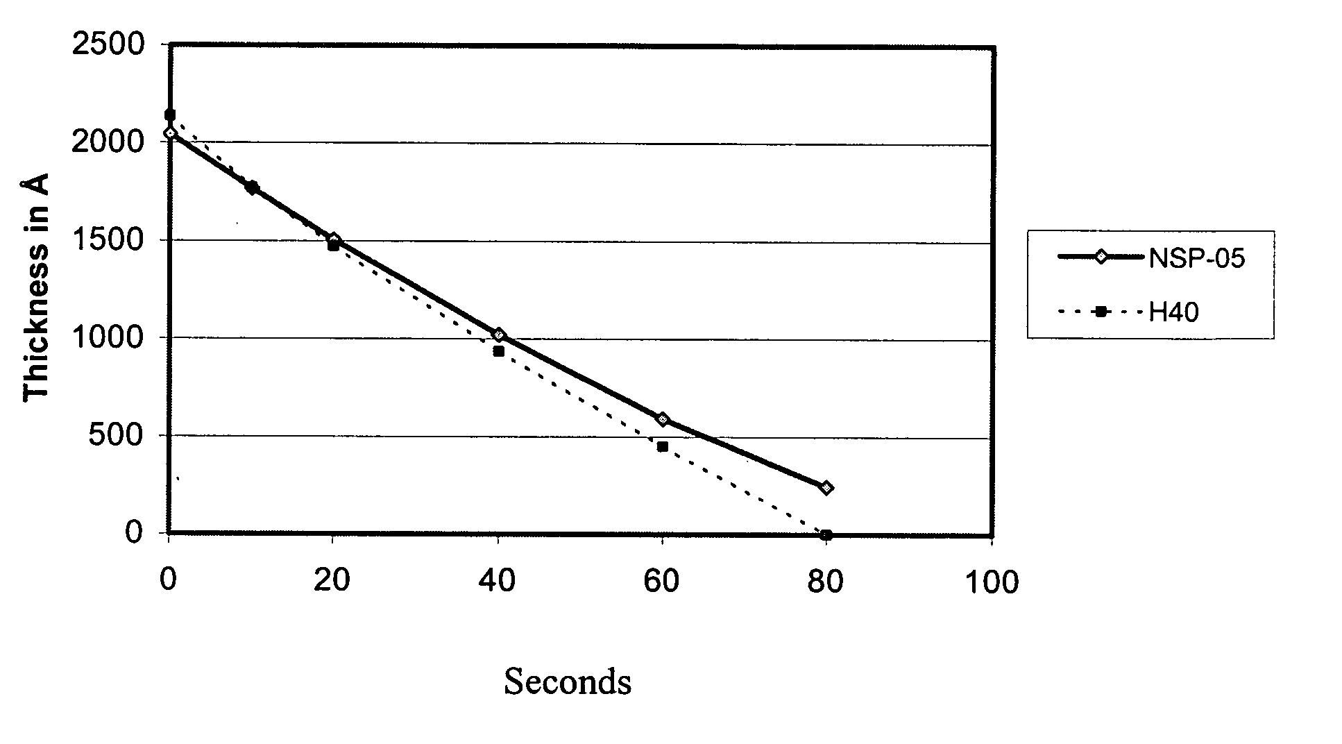
[0036] In this example, a gap fill material was prepared by mixing 5.65% by weight of BOLTORN H40 (a hyperbranched polymer having a molecular weight of 5100 g / mole and available from Perstorp Specialty Chemicals AB, Sweden), 0.05% by weight of CYMEL 303LF (a crosslinking agent available from Cytec Industries), 1.31% by weight of POWDERLINK 1174 (a crosslinking agent available from Cytec Industries), 0.018% by weight of p-toluenesulfonic acid (pTSA), 0.32% by weight of Bisphenol-A, 91.652% by weight of propylene glycol monomethyl ether (PGME), and 1.0% by weight of propylene glycol monomethyl ether acetate (PGMEA). The solution was coated onto a silicon wafer at 1500 rpm for 60 seconds and then baked at 205° C. for 60 seconds. The film thickness was 190 nm measured on an ellipsometer. The refractive index, n, was 1.60 at a wavelength of 248 m and 1.71 at a wavelength of 193 nm. The extinction coefficient, k...

example 2

Formulation of Gap Fill Material for Exposure Wavelengths of Less Than 400 nm

[0037] In this example, a gap fill material was prepared by mixing 5.65% by weight of BOLTORN H20 (a hyperbranched polymer having a molecular weight of 5100 g / mole and available from Perstorp Specialty Chemicals AB, Sweden), 0.05% by weight of CYMEL 303LF, 1.31% by weight of POWDERLINK 1174, 0.018% by weight of pTSA, 0.32% by weight of Bisphenol-A, 91.652% by weight of PGME, and 1.0% by weight of PGMEA. The solution was coated onto a silicon wafer at 1500 rpm for 60 seconds and then baked at 205° C. for 60 seconds. The film thickness was 183 nm measured on an ellipsometer. The refractive index, n, was 1.60 at a wavelength of 248 nm and 1.70 at a wavelength of 193 nm. The extinction coefficient, k, was 0.00 at a wavelength of 248 nm and 0.05 at a wavelength of 193 mm.

example 3

Formulation of Gap Fill Material for Exposure Wavelengths of Less Than 400 nm

[0038] In this example, a gap fill material was prepared by mixing 5.65% by weight of BOLTORN H30 (a hyperbranched polymer having a molecular weight of 5100 g / mole and available from Perstorp Specialty Chemicals AB, Sweden), 0.05% by weight of CYMEL 303LF, 1.31% by weight of POWDERLINK 1174, 0.018% by weight of pTSA, 0.32% by weight of Bisphenol-A, 91.652% by weight of PGME, and 1.0% by weight of PGMEA. The solution was coated onto a silicon wafer at 1500 rpm for 60 seconds and then baked at 205° C. for 60 seconds. The film thickness was 186 nm measured on an ellipsometer. The refractive index, n, was 1.60 at a wavelength of 248 nm and 1.70 at a wavelength of 193 nm. The extinction coefficient, k, was 0.01 at a wavelength of 248 nm and 0.05 at a wavelength of 193 mm.


PUM

PropertyMeasurementUnit
Temperatureaaaaaaaaaa
Fractionaaaaaaaaaa
Percent by massaaaaaaaaaa

Abstract

New anti-reflective or fill compositions having improved flow properties are provided. The compositions comprise a dendritic polymer dispersed or dissolved in a solvent system, and preferably a light attenuating compound, a crosslinking agent, and a catalyst. The inventive compositions can be used to protect contact or via holes from degradation during subsequent etching in the dual damascene process. The inventive compositions can also be applied to substrates (e.g., silicon wafers) to form anti-reflective coating layers having high etch rates which minimize or prevent reflection during subsequent photoresist exposure and developing.

Description

BACKGROUND OF THE INVENTION [0001] 1. Field of the Invention [0002] The present invention is concerned with new anti-reflective compositions and via fill compositions for use in the manufacture of microelectronic devices. These compositions include a dendritic polymer dispersed or dissolved in a solvent system. [0003] 2. Description of the Prior Art 1. Anti-reflective Coatings [0004] Integrated circuit manufacturers are consistently seeking to maximize substrate wafer sizes and minimize device feature dimensions in order to improve yield, reduce unit case, and increase on-chip computing power. Device feature sizes on silicon or other chips are now submicron in size with the advent of advanced deep ultraviolet (DUV) microlithographic processes. [0005] However, a frequent problem encountered by photoresists during the manufacturing of semiconductor devices is that activating radiation is reflected back into the photoresist by the substrate on which it is supported. Such reflectivity ...

Claims


Application Information

Patent Timeline
IPC IPC(8): C08K5/15
CPCC09D5/34Y10T428/2462C09D201/005
Inventor DEVADOSS, CHELLADURALBHAVE, MANDARHUANG, RUNHUL
Owner BREWER SCI
Why Eureka
Try Eureka