
Printed circuit board including embedded chips and method of fabricating the same

Inactive Publication Date: 2006-07-20
SAMSUNG ELECTRO MECHANICS CO LTD
View PDF4 Cites 24 Cited by
  • Summary
  • Abstract
  • Description
  • Claims
  • Application Information

AI Technical Summary

Benefits of technology

[0047] Accordingly, the present invention has been made keeping in mind the above problems occurring in the related art, and an object of the present invention is to provide a multi-layered PCB including embedded chips, and a method of fabricating the same, in which interlayer electrical connection is realized while constitutive layers of the PCB having chips such as active and passive components are simultaneously laminated, thereby drastically decreasing the number of processes.

Problems solved by technology

However, as the speed of the component increases, voltage fluctuation of a power line occurs, resulting in the generation of a lot of high frequency noise, such as SSN (Simultaneous Switching Noise) or delta-I (ΔI).
The high frequency noise (e.g., SSN) causes system delay or a logic fault, thereby decreasing the performance and reliability of the system.
In such cases, the first and second conventional techniques are disadvantageous because the space between the electrical component and the insulating layer as the central layer is large, and thus, the resultant product has a large size.
Further, the first and second conventional techniques are disadvantageous because the space between the chip and the copper foil layer is large, and thus, efficient radiating effects cannot be obtained.
Furthermore, the second conventional technique is disadvantageous because a build-up process used for lamination takes a long time.
However, the third conventional technique is disadvantageous in that because the through holes filled with conductive ink adhere to the chip upon simultaneous lamination, the alignment of the layers cannot be accurately controlled.
Moreover, since the radiation takes place using the radiating pattern, limitations are imposed on fabricating a high density circuit due to the formation of a passage required for emission of the radiating pattern.

Method used


Image

  • Printed circuit board including embedded chips and method of fabricating the same
  • Printed circuit board including embedded chips and method of fabricating the same
  • Printed circuit board including embedded chips and method of fabricating the same

Examples


Embodiment Construction

[0065] Hereinafter, embodiments of the present invention are described, with reference to the appended drawings.

[0066]FIGS. 4a to 4d sequentially show a process of fabricating a circuit layer of a PCB including embedded chips, according to an embodiment of the present invention.

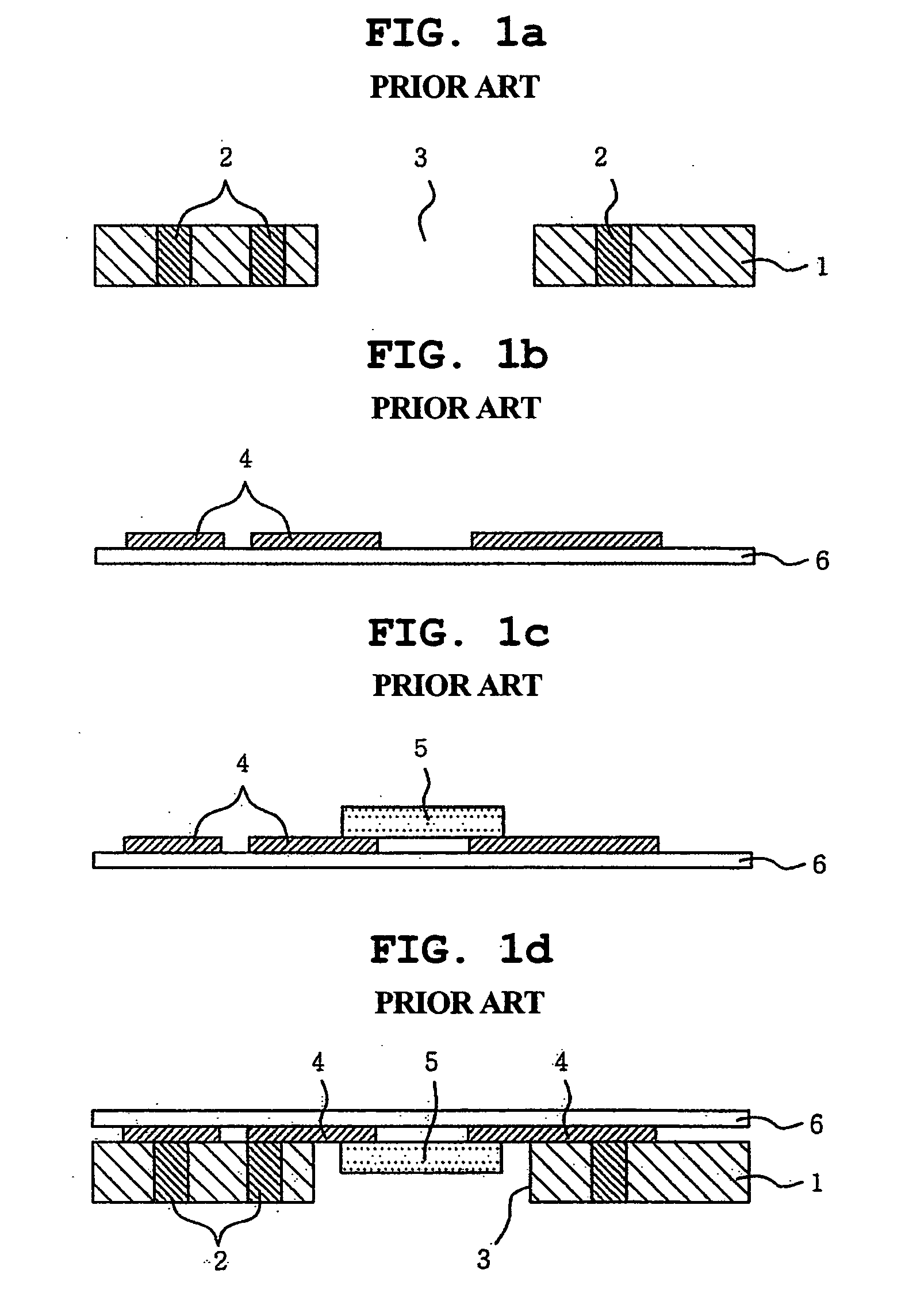
[0067] In FIG. 4a, a copper clad laminate (CCL) having an insulating resin layer 101 and copper foil layers 102a and 102b formed on both surfaces thereof is prepared.

[0068] In this case, the CCL having the insulating resin layer 101 and the copper foil layers 102a and 102b formed on both surfaces thereof is exemplified by glass / epoxy CCLs, heat resistant resin CCLs, paper / phenol CCLs, high frequency CCLs, flexible CCLs, complex CCLs, etc., depending on its uses.

[0069] In FIG. 4b, an etching resist 103 is applied on one surface of the CCL having the insulating resin layer 101 and the copper foil layers 102a and 102b formed on both surfaces thereof, and then exposed to light, to form an etching resist patte...


PUM


Abstract

A printed circuit board having embedded chips, composed of a central layer having an embedded chip, an insulating layer formed on one surface or both surfaces of the central layer and having a via hole filled with conductive ink, and a circuit layer formed on the insulating layer and having a via hole and a circuit pattern electrically connected to the chip of the central layer through the via hole of the insulating layer. In addition, a method of fabricating a printed circuit board including embedded chips is provided.

Description

INCORPORATION BY REFERENCE [0001] The present application claims priority under 35 U.S.C. §119 to Korean Patent Application No. 2004-116805 filed on Dec. 30, 2004. The content of the application is incorporated herein by reference in its entirety. BACKGROUND OF THE INVENTION [0002] 1. Field of the Invention [0003] The present invention relates, generally, to a printed circuit board (PCB) including embedded chips, and a fabricating method thereof. More particularly, the present invention relates to a PCB including embedded chips, which comprises a central layer having an embedded chip, an insulating layer formed on one surface or both surfaces of the central layer and having a through hole filled with conductive ink, and a circuit layer formed on the insulating layer and having a via hole and a circuit pattern electrically connected to the chip of the central layer through the through hole of the insulating layer, and a method of fabricating such a PCB. The method of fabricating the ...

Claims


Application Information

Patent Timeline
IPC IPC(8): H01L23/02
CPCH01L23/5389H01L25/0655H01L25/16H01L2224/82039H01L2924/01078H01L2924/01087H05K1/186H05K3/4069H05K3/4602H05K3/4614H05K3/4652H05K2201/09563H05K2201/10674H05K2203/0191H05K1/18H05K3/30
Inventor RYU, CHANGLEE, DOOAHN, JINKANG, MYUNGCHO, SUK
Owner SAMSUNG ELECTRO MECHANICS CO LTD
Features
  • Generate Ideas
  • Intellectual Property
  • Life Sciences
  • Materials
  • Tech Scout
  • Unparalleled Data Quality
  • Higher Quality Content
  • 60% Fewer Hallucinations
Learn More