Semiconductor device

a technology of semiconductor devices and semiconductors, applied in the direction of information storage, static storage, digital storage, etc., can solve the problems of destroying stored data in peripheral memory elements, joule heat damage to data in elements, and generating thermal disturbances larger than expected, so as to improve read-out operations and stable generation of reference voltages

Active Publication Date: 2006-07-20
RENESAS ELECTRONICS CORP
View PDF4 Cites 27 Cited by
  • Summary
  • Abstract
  • Description
  • Claims
  • Application Information

AI Technical Summary

Benefits of technology

[0019] It should be noted that the above-described effects are particularly advantageous in the case where the storage elements of the memory cells are variable resistive elements of, for example, a chalcogenide material.
[0020] The effects obtained by ty

Problems solved by technology

On the other hand, in the read-out operation, since a current is caused to flow through the element or the adjacent heater, the data in the element may be destroyed by Joule heat generated by the current.
Also, there is a possibility that, when a read current flows, a thermal disturbance larger than expected is generated due to the influen

Method used


Image

  • Semiconductor device
  • Semiconductor device
  • Semiconductor device

Examples


first embodiment

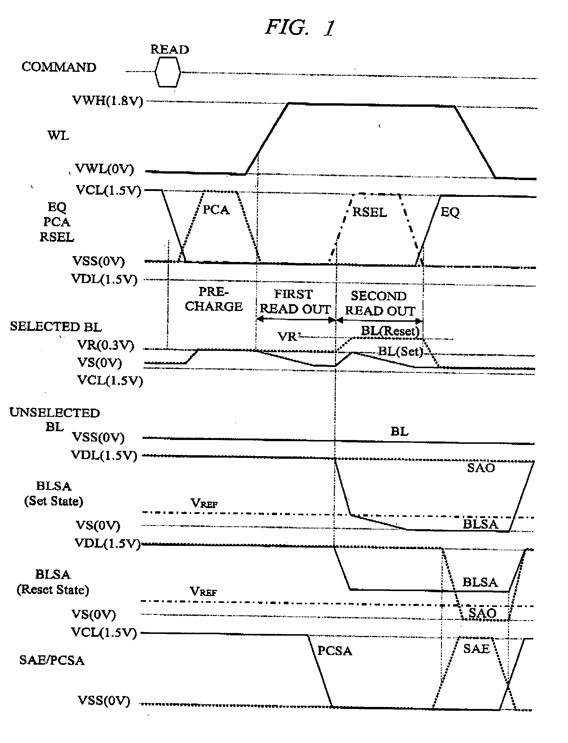
[0059]FIG. 1 is a waveform diagram showing an example of a read-out operation of a phase change memory which is included in a semiconductor device according to a first embodiment of the present invention. This read-out operation is characterized in that a low voltage is applied (precharged) to a bit line at the beginning of the read-out operation, and after performing a read-out operation (first read out), charge is injected into the read bit line by sharing the charge with a sense amplifier so as to perform a read-out operation again (second read out).

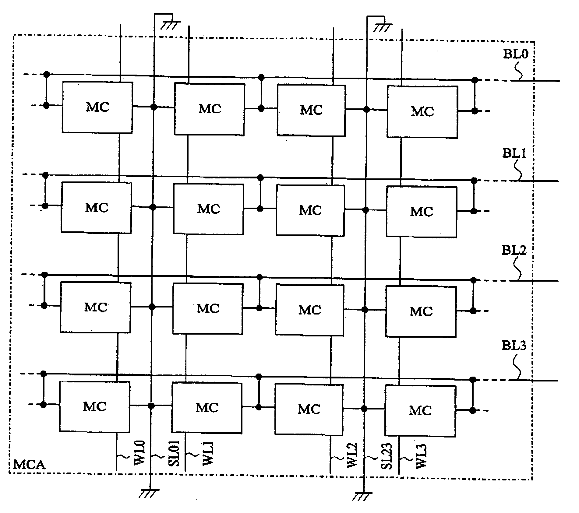
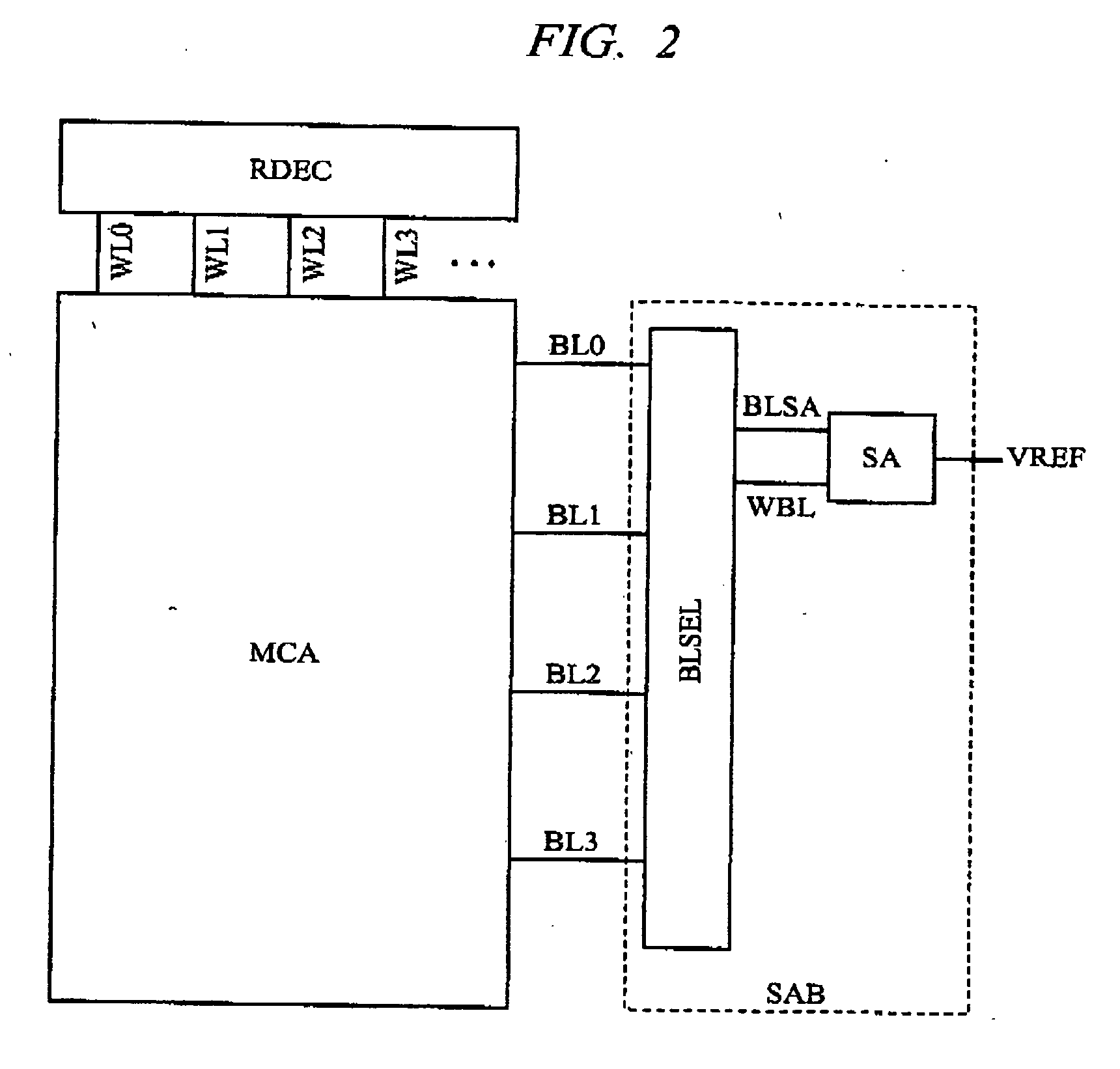
[0060] Before describing details of the operation, circuit configurations for realizing the present read-out operation will be described below. FIG. 2 is a block diagram showing a configuration example of a main part of the phase change memory which is included in the semiconductor device according to the first embodiment of the present invention. The configuration example shown in FIG. 2 is formed on a semiconductor substrate and in...

second embodiment

[0115] In a second embodiment, a method of generating the reference level in a read-out period will be described with using the above-described configurations and operations. Characteristics of the present method are that the time in which a high voltage is applied during a read-out period is shortened while increasing the read-out signal amount by performing a read out in two steps similar to the above-described read-out operation, and a stable reference level is generated by outputting the reference level by charge sharing. First, circuit configurations for realizing the present read-out operation will be described.

[0116]FIG. 19 is a block diagram showing a configuration example of a main part of the phase change memory included in a semiconductor device according to the second embodiment of the present invention. FIG. 19 shows the memory cell array MCA, the row decoder RDEC for selecting the word lines WL corresponding to inputted addresses, and the sense amplifier block SAB for...


PUM


Abstract

In a semiconductor device particularly including a phase change material, the reliability of the read-out operation is improved. In a read-out operation of a phase change memory, a bit line to be read out is precharged in advance with a sufficiently low voltage that can prevent the destructive read operation. In this state, after a word line is activated and a period in which the voltage is sufficiently discharged via a storage element which is in a low resistance state elapses (first read out), charge sharing is performed between the bit line and a read bit line of a sense amplifier which is precharged to a high voltage, and a read-out operation is performed again (second read out). Consequently, the read-out signal amount can be increased while suppressing the read current.

Description

CROSS-REFERENCE TO RELATED APPLICATION [0001] The present application claims priority from Japanese Patent Application No. JP 2004-374314 filed on Dec. 24, 2004, the content of which is hereby incorporated by reference into this application. TECHNICAL FIELD OF THE INVENTION [0002] The present invention relates to a semiconductor device. More particularly, it relates to a technology effectively applied to a semiconductor device having an integrated memory circuit, a logic-embedded memory in which memory circuits and logic circuits are provided on one semiconductor substrate, or an analog circuit, each of which is formed by using a phase change material. BACKGROUND OF THE INVENTION [0003] According to an examination by the inventor of the present invention, the followings are known as the technologies for a memory using a phase change material. [0004] Phase change memories have been under development in order to produce high-speed and large-scale integrated non-volatile memories. A me...

Claims


Application Information

Patent Timeline
IPC IPC(8): G11C11/00
CPCG11C7/12G11C13/0004G11C13/0026G11C13/004G11C2013/0054G11C2013/0057
Inventor TAKEMURA, RIICHIRO
Owner RENESAS ELECTRONICS CORP
Why Eureka
Try Eureka