Photonic integrated circuit

a photonic integrated circuit and integrated circuit technology, applied in the direction of optical waveguide light guide, instruments, nanotechnology, etc., to achieve the effect of improving the transfer efficiency of optical signals within the photonic crystal, reducing the loss of optical signals to the substrate or other higher refractive index supporting layer, and improving the transfer efficiency of optical fibers to the photonic circui

Inactive Publication Date: 2006-07-20
ENERGY CONVERSION DEVICES INC
View PDF7 Cites 28 Cited by
  • Summary
  • Abstract
  • Description
  • Claims
  • Application Information

AI Technical Summary

Benefits of technology

[0016] In other embodiments, the optical bench includes an undercut region located beneath a portion of the photonic circuit. The undercut region is formed by etching or otherwise removing a portion of the substrate or other supporting material upon which the photonic circuit is formed. In a preferred embodiment, the undercut region is contiguous with the trench formed in the optical bench and extends beneath the end of the photonic circuit in closest proximity to the optical fiber. Upon formation of an undercut region, the undercut portion of the photonic circuit protrudes into the trench and is surrounded by a medium that has a lower refractive index than the substrate or supporting material removed during the undercut process. In one embodiment, the surrounding medium is air and the undercut portion of the photonic circuit lacks mechanical support in the vertical direction. By surrounding the undercut portion of the photonic circuit with a low refractive index medium, the confinement of an optical signal within the photonic crystal is improved and losses of the optical signal to the substrate or other higher refractive index supporting layers is reduced. As a result, the transfer efficiency from an optical fiber to the photonic circuit is improved.
[0017] In another embodiment, the instant photonic platform includes an impedance matching photonic coupling device that facilitates the transfer from an optical fiber to the photonic circuit. The photonic coupling device is positioned between the optical fiber and the photonic circuit and enables high transfer efficiency by maintaining a constant or approximately constant optical impedance along the direction of propagation of the optical signal.

Problems solved by technology

Key issues include alignment of the fiber core with a planar waveguide or planar photonic crystal and minimization of transfer losses at the junction between the optical fiber and planar structure.

Method used


Image

  • Photonic integrated circuit
  • Photonic integrated circuit
  • Photonic integrated circuit

Examples


Embodiment Construction

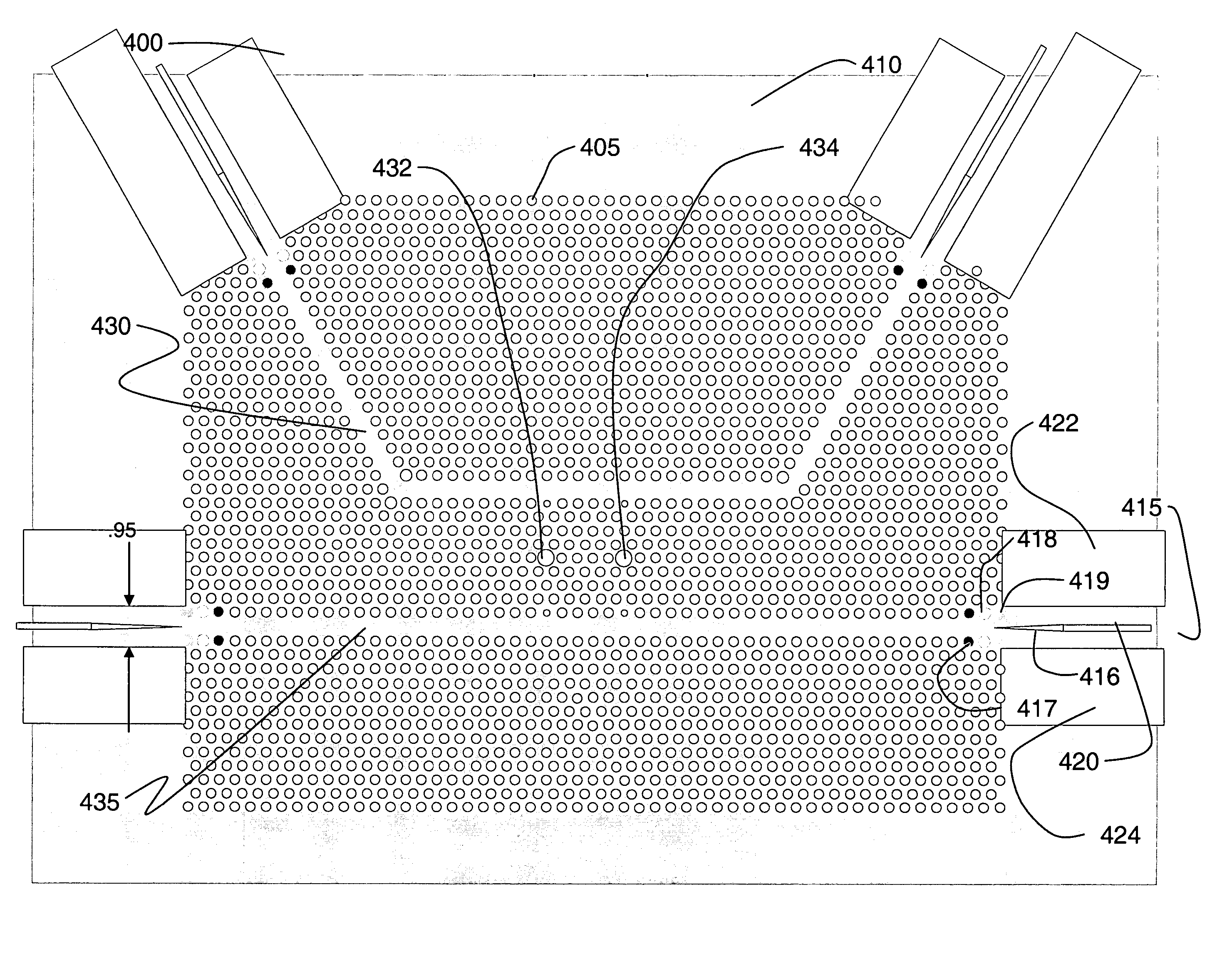
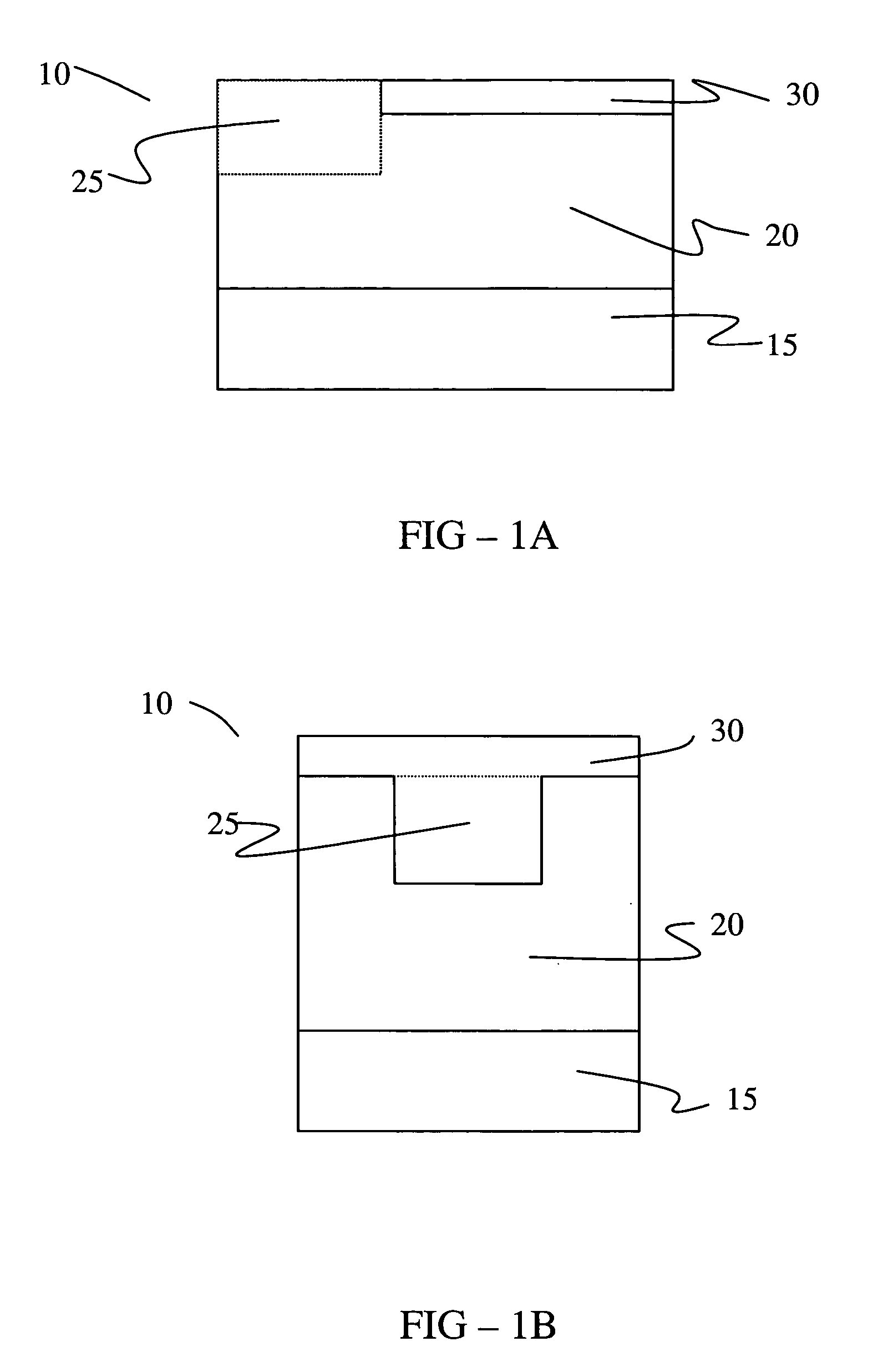
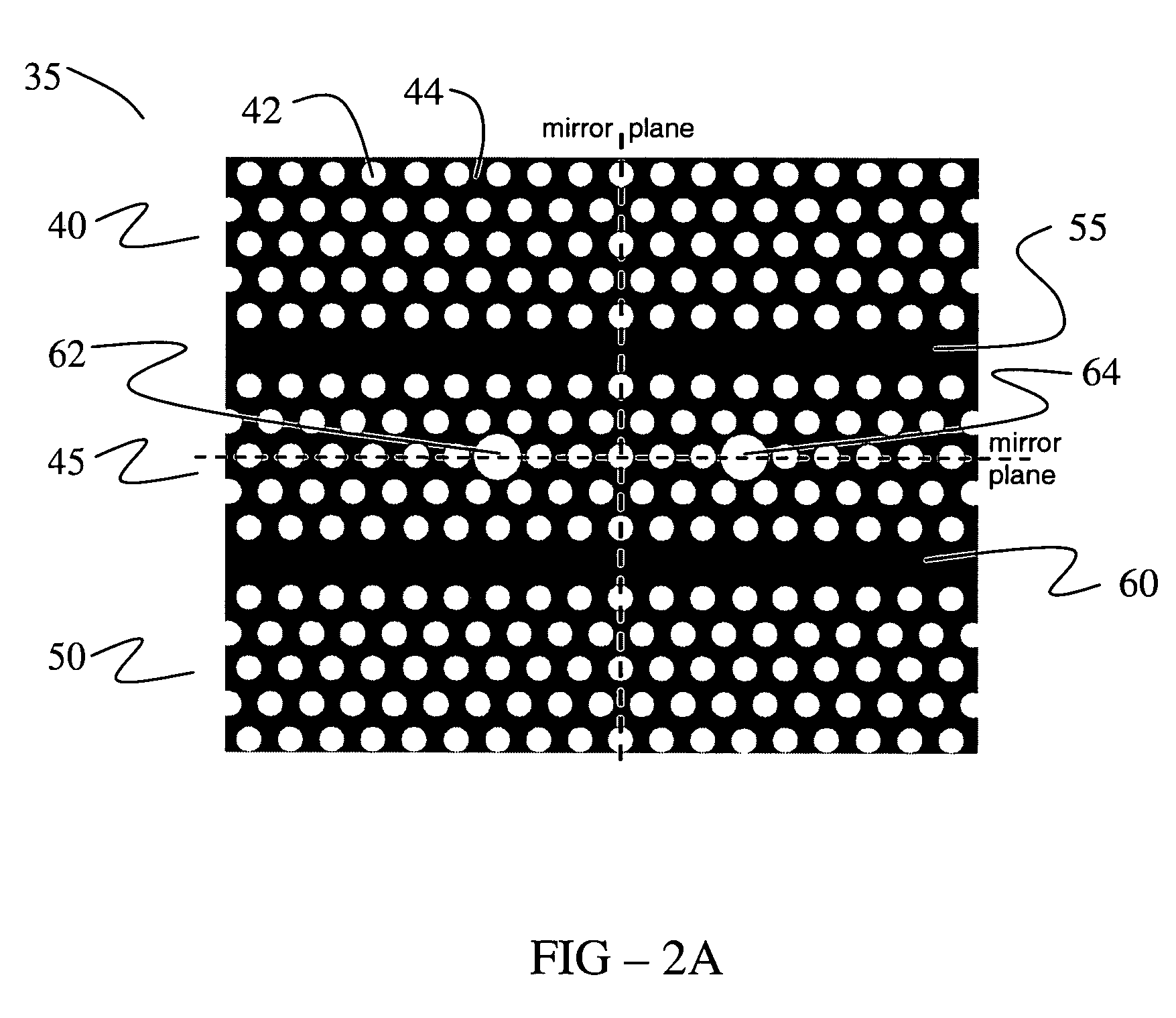
[0039] The realization of all-optical information networks requires the development of novel active and passive photonic devices, interconnection of those devices to form photonic circuits, and integration of photonic circuits with optical fibers. Envisioned optical networks include local nodes and a capacity to transfer optical signals to and from the local nodes. In most designs, optical fibers are the preferred medium for transmitting optical signals between nodes. The processing of optical signals typically occurs at the node level, where functions such as multiplexing, demultiplexing, steering, wavelength separation, and wavelength conversion occur. In order to achieve more sophisticated processing of optical signals, it is necessary to improve the level of control over the wavelength, direction of propagation, intensity, and mode characteristics of individual optical signals and to combine and separate multiple optical signals to provide multichannel capability and high throug...


PUM


Abstract

An optical platform including optical bench, an optical or photonic coupling device and a photonic circuit. The photonic circuit includes a photonic crystal along a waveguide and/or defect. The coupling device may be a waveguide or impedance matching interconnection device. The optical bench includes a rectangular trench to seat an optical fiber and provide alignment with the photonic circuit.

Description

CROSS-REFERENCE TO RELATED APPLICATIONS [0001] This application is a continuation in part of U.S. patent application Ser. No. 10 / 855,482, entitled “Optical Coupling Device” and filed on May 27, 2004, and a continuation in part of U.S. patent application Ser. No. 11 / 124,736, entitled “Photonic Coupling Device” and filed on May 9, 2005; the disclosures of which is hereby incorporated by reference herein.FIELD OF INVENTION [0002] This invention relates to integrated optical elements for the transmission and direction of light in an optical circuit. More specifically, this invention relates to a platform that includes a photonic circuit and an optical bench that permits the efficient coupling of optical fibers to photonic devices such as photonic crystals and waveguides. Most specifically, this invention relates to an optical bench that includes a trench region to accommodate an optical fiber in such way that optimal alignment and index matching occurs with the photonic circuit to provi...

Claims


Application Information

Patent Timeline
Patent Type & Authority Applications(United States)
IPC IPC(8): G02B6/10G02B6/26G02B6/42G02B6/12
CPCB82Y20/00G02B6/12004G02B6/1225G02B6/3692G02B6/305G02B6/3652G02B6/30
Inventor MILLER, ROBERT A.
Owner ENERGY CONVERSION DEVICES INC
Why Eureka
Try Eureka