Measuring apparatus

a technology of measuring apparatus and measuring plate, which is applied in the direction of instruments, semiconductor/solid-state device testing/measurement, flaw detection using microwaves, etc., can solve the problems of large loss, short circuit, metal interconnects under the insulating layer may be exposed, etc., and achieve accurate measurement and reduce fabrication costs

Inactive Publication Date: 2006-07-27
EBARA CORP
View PDF10 Cites 38 Cited by
  • Summary
  • Abstract
  • Description
  • Claims
  • Application Information

AI Technical Summary

Benefits of technology

[0022] According to the present invention, even if an obstacle (e.g., a polishing pad) exists between the substance as an object to be measured and the microwave emission device, the microwave passes (penetrates) through the obstacle to reach the substance (e.g., a substrate). Therefore, it is not necessary to provide a transmitting window such as a through-hole in the obstacle. As a result, a process for providing such a transmitting window is not required, and hence the fabrication cost can be reduced. Further, according to the present invention, a thickness or the like of the substance can be measured accurately without being affected by a polishing liquid or the like.

Problems solved by technology

In such a case, if the insulating layer is excessively polished, then the metal interconnects underneath the insulating layer may be exposed.
In this case, if the polishing process is excessively performed to polish the Cu layer in the interconnect grooves together with the insulating layer, a circuit resistance becomes large, and hence the semiconductor device should be discarded, resulting in a large loss.
In contrast thereto, if the polishing process is not sufficiently performed to allow the Cu layer to remain on the insulating layer, the circuit interconnects are not divided from each other, thus causing a short circuit.
As a result, the polishing process should be performed again, and hence a fabrication cost is increased.
Such a problem occurs not only in case of polishing the Cu layer, but also in case of polishing other kinds of metal layers such as Al layer by the CMP process after forming such a metal layer.
However, the above-mentioned measuring apparatuses have the following problems: If an obstacle such as a polishing pad exists between the light source and the semiconductor wafer, the laser beam and the visible ray emitted from the light source cannot reach the semiconductor wafer.
As a result, the number of fabrication processes of the polishing pad is increased, and hence the fabrication cost of the polishing pad as an expendable component is increased.
Further, in the above-mentioned measuring apparatus, the reflected laser beam and the reflected visible ray from the semiconductor wafer are unstable.
Therefore, it is difficult to accurately measure a film thickness.

Method used


Image

  • Measuring apparatus
  • Measuring apparatus
  • Measuring apparatus

Examples


first embodiment

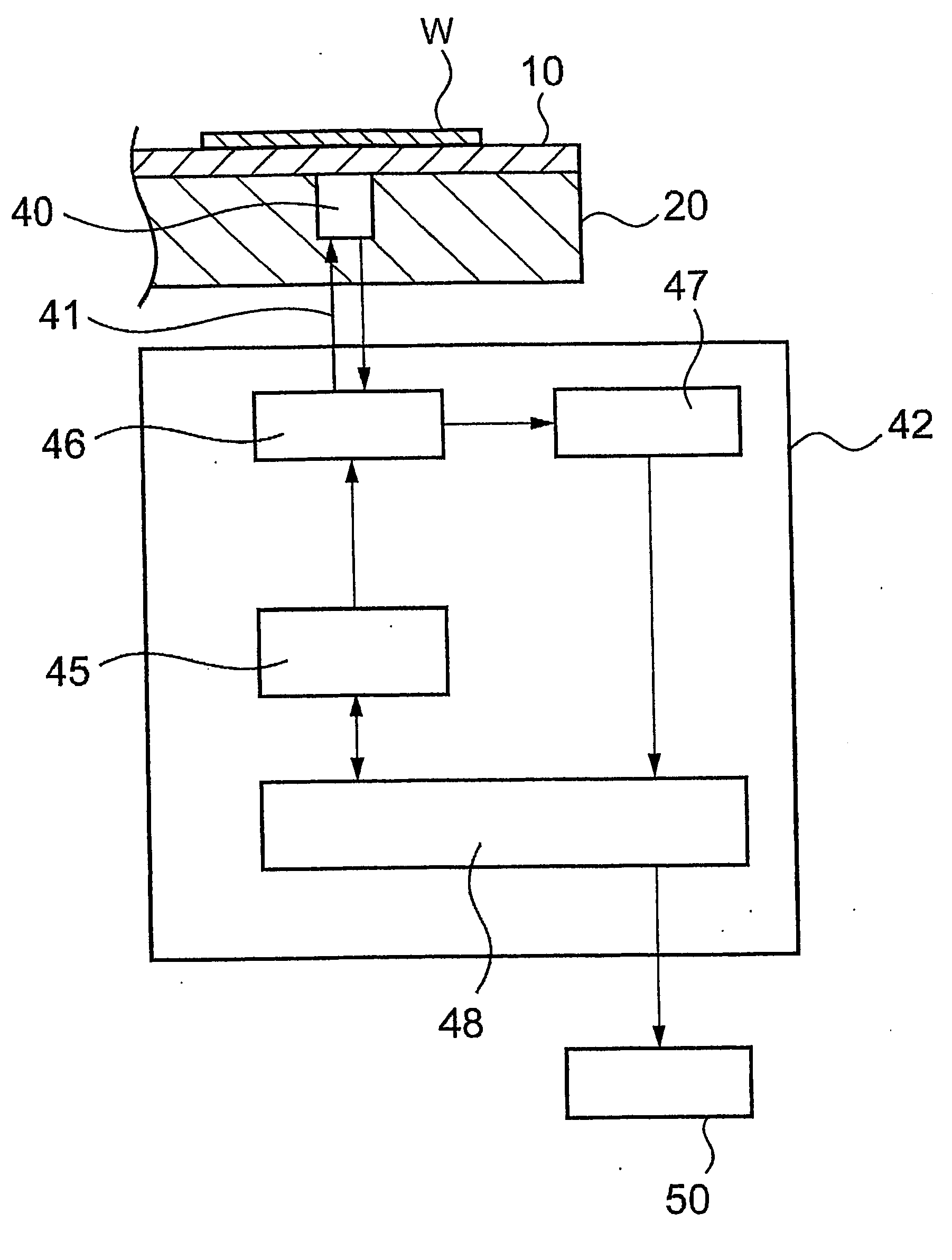
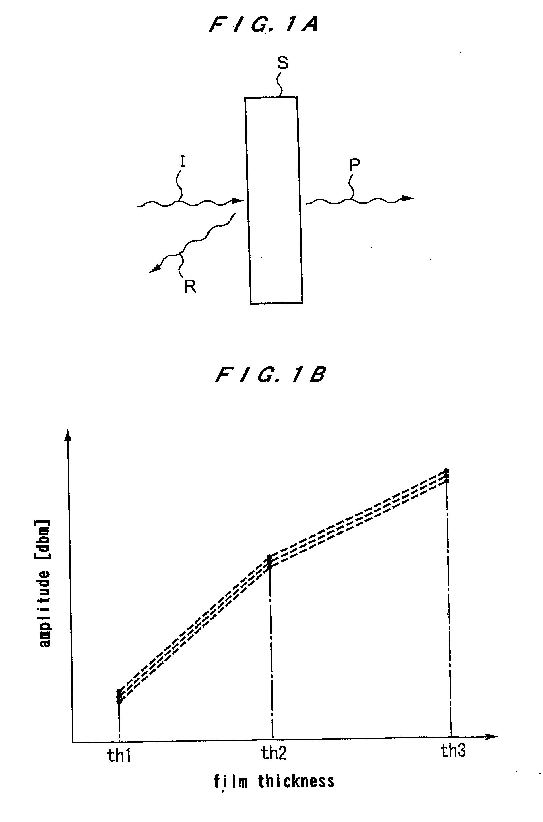
[0041] A measuring apparatus according to embodiments of the present invention will be described below with reference to the drawings. FIG. 1A is a view illustrating a principle of a measuring apparatus according to the present invention. As shown in FIG. 1A, when a microwave (an incident wave I) is emitted to a substance S to be measured, the microwave is reflected by the substance S. The reflected microwave from the substance S (hereinafter referred to as a reflected wave R) has an amplitude and a phase which have varied depending on a structure such as a thickness and a physical property of the substance S. Therefore, the structure of the substance S can be analyzed by detecting at least one of the amplitude and the phase of the reflected wave R. The structure of the substance includes a thickness of the substance, an internal defect such as void formed in the substance, a dielectric constant, an electric conductivity, and a magnetic permeability.

[0042] For example, if a thicknes...

second embodiment

[0098] Next, a measuring method and a measuring apparatus of the present invention will be described in detail.

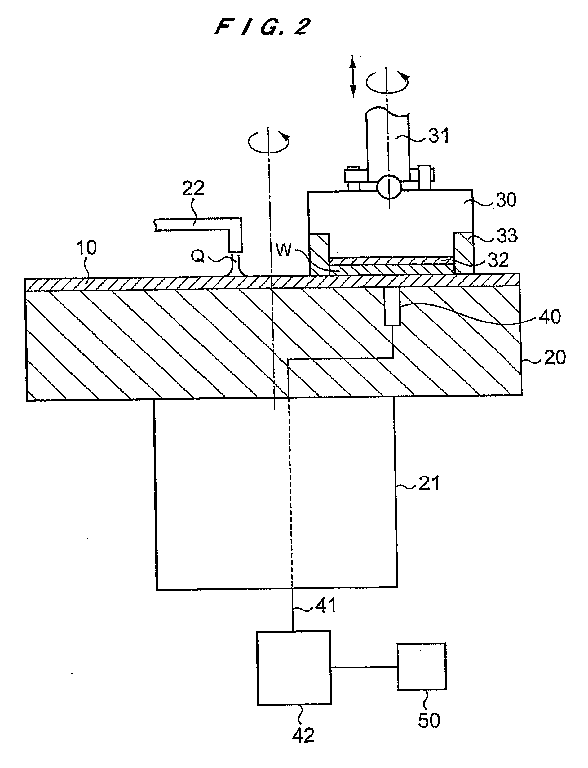
[0099] In this embodiment, a microwave is used as an electromagnetic wave to be emitted to a substance. Preferably, a millimeter wave having a frequency in the range of 30 to 300 GHz and a wave length in the range of 10 to 1 mm is used. Further, in order to enhance a S / N ratio and perform a quick measurement, an amplitude-modulated electromagnetic wave is preferably used. In this embodiment, the electromagnetic wave to be emitted to the substance is a linearly polarized wave or a circularly polarized wave, which is incident obliquely to the substance. In a case of using the linearly polarized wave, a direction of an electric field vector thereof is inclined at an angle of 45° in a clockwise or a counter-clockwise direction with respect to a plane perpendicular to a plane of incident.

[0100] Generally, in ellipsometry, a receive detector (i.e., a set of a receiving antenna a...


PUM

PropertyMeasurementUnit
wave lengthaaaaaaaaaa
frequencyaaaaaaaaaa
wave lengthaaaaaaaaaa

Abstract

The present invention relates to a measuring apparatus for measuring a thickness or the like of a thin film formed on a surface of a substrate such as a semiconductor wafer. The measuring apparatus includes a microwave emission device (40) for emitting a microwave to a substance, a microwave generator (45) for supplying the microwave to the microwave emission device (40), a detector (47) for detecting an amplitude or a phase of the microwave which has been reflected from or passed through the substance, and an analyzer (48) for analyzing a structure of the substance based on the amplitude or the phase of the microwave which has been detected by the detector (47).

Description

TECHNICAL FIELD [0001] The present invention relates to a measuring apparatus for measuring a thickness or the like of a substance, and more particularly to a measuring apparatus for measuring a thickness or the like of a thin film formed on a surface of a substrate such as a semiconductor wafer. BACKGROUND ART [0002] As semiconductor devices have become more highly integrated in recent years, circuit interconnects have been required to be finer, and the number of layers in multilayer interconnects has been increased. Under such a tendency, there has been a demand for planarizing a surface of a substrate such as a semiconductor wafer. Specifically, as the circuit interconnects become finer, a wave length of a light used in a photolithography becomes shorter. In case of using such a light having a short wave length, step heights that can be allowed in focus regions on the surface of the substrate become smaller. Thus, a highly flat surface is required for the substrate so that the st...

Claims


Application Information

Patent Timeline
Patent Type & Authority Applications(United States)
IPC IPC(8): G01R27/04G01B15/02G01N22/00
CPCG01B15/02G01N22/00G01N22/02H01L22/00
Inventor TADA, MITSUOSUTO, YASUNARI
Owner EBARA CORP
Why Eureka
Try Eureka