
SiCOH dielectric material with improved toughness and improved Si-C bonding, semiconductor device containing the same, and method to make the same

a dielectric material and toughness technology, applied in the direction of radiation control devices, transportation and packaging, coatings, etc., can solve the problems of increased signal delay in ulsi electronic devices, low cohesive strength, low elongation to break, etc., to improve the resistance and resistance of ulsi electronic devices, the effect of reducing the slope and small slop

Inactive Publication Date: 2006-07-27
INTEL CORP
View PDF37 Cites 35 Cited by
  • Summary
  • Abstract
  • Description
  • Claims
  • Application Information

AI Technical Summary

Benefits of technology

The new SiCOH dielectric material exhibits significantly increased cohesive strength, reduced environmental sensitivity, and improved resistance to water degradation, enabling its use in ULSI devices with enhanced reliability and performance.

Problems solved by technology

This combined effect increases signal delays in ULSI electronic devices.
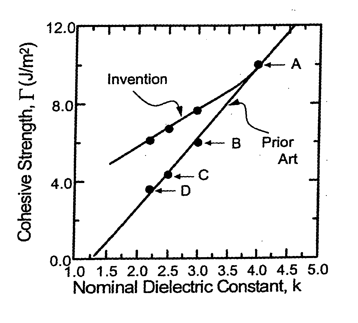
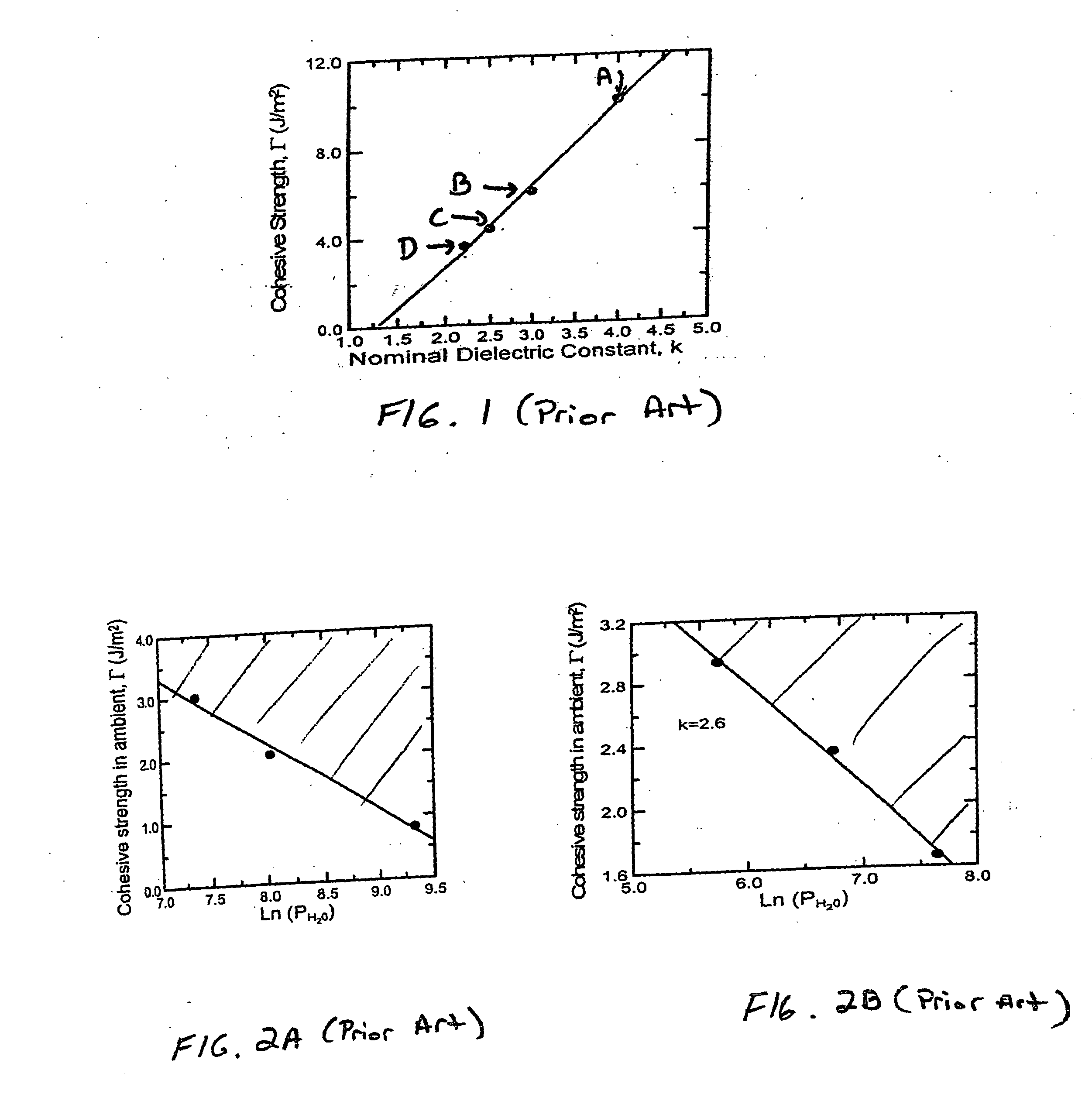
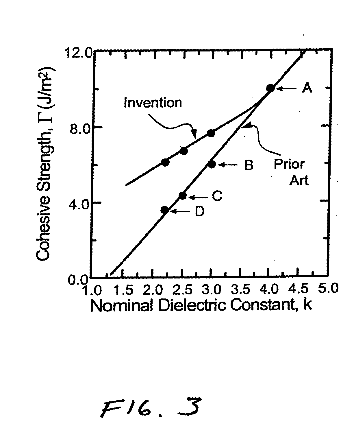
Key problems with prior art ultra low k SiCOH films include, for example: (a) they are brittle (i.e., low cohesive strength, low elongation to break, low fracture toughness); (b) liquid water and water vapor reduce the cohesive strength of the material even further.
Another problem with prior art SiCOH films is that their strength tends to be degraded by H2O.
Addition of more organic polymer content to SiCOH will lead to a dielectric with increased fracture toughness and decreased environmental sensitivity.

Method used


Image

  • SiCOH dielectric material with improved toughness and improved Si-C bonding, semiconductor device containing the same, and method to make the same
  • SiCOH dielectric material with improved toughness and improved Si-C bonding, semiconductor device containing the same, and method to make the same
  • SiCOH dielectric material with improved toughness and improved Si-C bonding, semiconductor device containing the same, and method to make the same

Examples


example 1

SiCOH material A

[0084] In this example, an inventive SiCOH dielectric, referred to as SiCOH film A, which was made in accordance with the present invention, was characterized by the data in FIG. 5 and in Table 1 below. For comparison, SiCOH films B and C are “typical” prior art SiCOH films, that have a dielectric constant about 2.7-2.8 are also shown in FIG. 5 and Table 1.

[0085] Referring to FIG. 5, this figure shows solid-state NMR (nuclear magnetic resonance) spectra for the 13C nuclei for the film SiCOH film A. Peak 33 corresponds to 13C for CH3 methyl groups bonded to Si, and the breadth of peak 33 is due to CH3 groups in different magnetic environments. The peak 32 was assigned to 13C in —CH2— species, bridging between two Si atoms, Si—CH2—Si. Based on the height of peak 32, the fraction of the total C in the film that is C present as methylene bridge groups, —CH2— was about 0.1. Since peaks 33 and 32 were overlapping, this was an estimate only. The areas have not been measur...

example 2

First Process Embodiment

[0087] A 300 mm or 200 mm substrate was placed in a PECVD reactor on a heated wafer chuck at 350° C. Temperatures between 300°-425° C. may also be used. Any PECVD deposition reactor may be used within the present invention. Gas and liquid precursor flows were then stabilized to reach a pressure in the range from 0.1-10 Torr, and RF radiation was applied to the reactor showerhead for a time between about 5 to about 500 seconds.

[0088] Specifically and for the growth of the inventive SiCOH dielectric material A containing enhanced Si—CH2—Si bridging methylene carbon (described above), the single SiCOH precursor was OMCTS (octamethylcyclotetrasiloxane) set at a flow of 2500 mg / m, an oxygen, O2 flow of 220 sccm, a helium, He gas flow of 2000 sccm, said flows were stabilized to reach a reactor pressure of 5 Torr. The wafer chuck was set at 350° C., and the high frequency RF power of 400 W at a frequency of 13.6 MHz was applied to the showerhead, and the low frequ...

example 3

Second Process Embodiment

[0089] A 300 mm or 200 mm substrate was placed in a PECVD reactor on a heated wafer chuck at 300°-425° C. and preferably at 350°-400° C. Any PECVD deposition reactor may be used within the present invention. Gas and liquid precursor flows were then stabilized to reach a pressure in the range from 0.1-10 Torr, and RF radiation was applied to the reactor showerhead for a time between about 5 to 500 seconds.

[0090] Specifically and for the growth of the inventive SiCOH dielectric containing enhanced Si—CH2—Si bridging methylene carbon (described above), the conditions used include: 1,1,1,3,3,3-hexamethoxy-1,3-disilapropane, flow of 2500 mg / m, an oxygen, O2 flow of 220 sccm, a helium, He gas flow of 2000 sccm, said flows were stabilized to reach a reactor pressure of 5 Torr. The wafer chuck was set at 350° C., and the high frequency RF power of 500 W at a frequency of 13.6 MHz was applied to the showerhead, and the low frequency RF power of 160 W at a frequency...


PUM

PropertyMeasurementUnit
dielectric constantaaaaaaaaaa
temperatureaaaaaaaaaa
dielectric constantaaaaaaaaaa

Abstract

A low-k dielectric material with increased cohesive strength for use in electronic structures including interconnect and sensing structures is provided that includes atoms of Si, C, O, and H in which a fraction of the C atoms are bonded as Si—CH3 functional groups, and another fraction of the C atoms are bonded as Si—R—Si, wherein R is phenyl, —[CH2]n— where n is greater than or equal to 1, HC═CH, C≡CH2, C≡C or a [S]n linkage, where n is a defined above.

Description

RELATED APPLICATIONS [0001] The present application is a continuation-in-part application of U.S. Ser. No. 11 / 040,778, filed Jan. 21, 2005, which application is related to co-assigned U.S. Pat. Nos. 6,147,009, 6,312,793, 6,441,491, 6,437,443, 6,541,398, 6,479,110 B2, and 6,497,963, the contents of which are incorporated herein by reference. The present application is also related to co-pending and co-assigned U.S. patent application Ser. Nos. 10 / 174,749, filed Jun. 19, 2002, 10 / 340,000, filed Jan. 23, 2003 and 10 / 390,801, filed Mar. 18, 2003, the entire contents of each of the aforementioned U.S. patent applications are also incorporated herein by reference.FIELD OF THE INVENTION [0002] The present invention generally relates to a class of dielectric materials comprising Si, C, O and H atoms (SiCOH) that have a low dielectric constant (k), and methods for fabricating films of these materials and electronic devices containing such films. Such materials are also called C doped oxide (...

Claims


Application Information

Patent Timeline
Patent Type & Authority Applications(United States)
IPC IPC(8): C23C16/00B05D3/00H01L27/148H01L31/103
CPCH01L31/103Y10T428/31663
Inventor EDELSTEIN, DANIEL C.GATES, STEPHEN M.GRILL, ALFREDLANE, MICHAELLIN, QINGHUANGMILLER, ROBERT D.NEUMAYER, DEBORAH A.NGUYEN, SON VAN
Owner INTEL CORP
Learn More