
Single crystal wafer for semiconductor laser

a single crystal wafer and laser technology, applied in the field of single crystal wafers for semiconductor lasers, can solve the problems of deteriorating angle adjustment precision, difficult focus, deteriorating precision in alignment of mask patterns, etc., to improve the process yield in manufacturing ld chips, improve alignment accuracy, and improve the effect of alignment accuracy

Inactive Publication Date: 2006-08-03
HITACHI CABLE
View PDF5 Cites 4 Cited by
  • Summary
  • Abstract
  • Description
  • Claims
  • Application Information

AI Technical Summary

Benefits of technology

[0017] Accordingly, it is an object of the invention to solve the above problems, and to provide a single crystal wafer for a semiconductor laser, which can realize an improvement in a precision of an optical alignment of mask pattern using the cleavage surface as a reference, and an improvement in process yield.
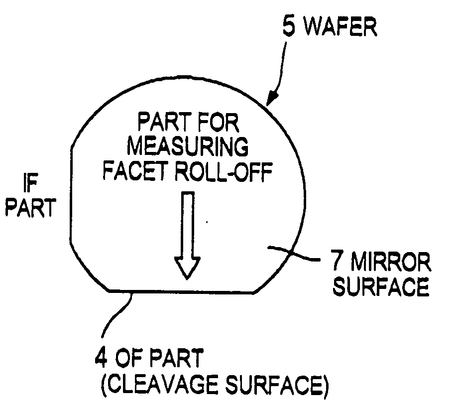
[0038] For solving the problem of deterioration of the alignment accuracy, the present invention provides a single crystal wafer for a semiconductor laser, in which a facet roll-off of a ridge of an OF cleavage surface is equal to or less than 40 μm, as a semiconductor wafer structure. In addition, for improving the alignment accuracy, it is more preferable to control the facet roll-off of the ridge of the OF cleavage surface to be smaller, i.e. equal to or less than 20 μm.
[0039] According to the present invention, a single crystal wafer for a semiconductor laser having a small facet roll-off of a ridge of an OF cleavage surface, e.g. equal to or less than 40 μm, can be provided as a wafer structure for semiconductor laser. According to this structure, it is possible to realize an improvement in alignment accuracy of mask pattern using an optical alignment method, and an improvement in a process yield in manufacturing the LD chip.

Problems solved by technology

In the conventional arts of forming the orientation flat (OF) itself, when the angle adjustment is conducted by using an optical method, e.g. by using the microscope, since a cross section of a ridge of the OF part is curved, it is difficult to focus a microscope observation image on the OF part in a state where the operator observes the OF part from a point of view beneath a mirror surface, so that a precision in angle adjustment is deteriorated.
However, these prior arts do not refer to a relationship between the aforementioned “polishing” process and a “facet roll-off” formed at the OF cleavage surface.
Such a variation of the polishing conditions causes the facet roll-off at an outer periphery of the wafer including the OF cleavage surface (D>40 μm, see FIGS. 3A and 3B), so that it becomes difficult to focus on the OF cleavage surface using the microscope in the alignment of the mask pattern, thereby deteriorating the precision in the alignment of the mask pattern.

Method used


Image

  • Single crystal wafer for semiconductor laser
  • Single crystal wafer for semiconductor laser
  • Single crystal wafer for semiconductor laser

Examples


embodiments

[0057] Next, a single crystal wafer for a semiconductor laser in embodiments according to the present invention will be explained.

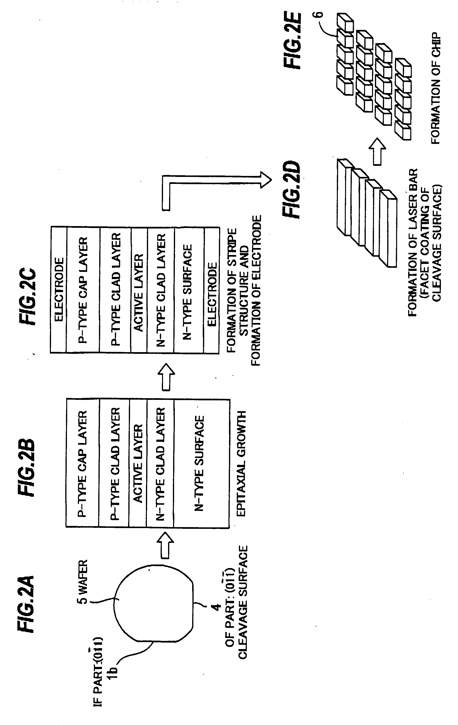
[0058] As shown in TABLE 1, a single crystal wafer for a semiconductor laser comprising of n-GaAs substrate having a diameter of 7.62 cm (3 inches) is manufactured according to a comparative example, first embodiment, and second embodiment, respectively, in which the three parameters of the polishing conditions (hardness of abrasive cloth, polishing rate, and pressure of pushing wafer) are changed, respectively. Then, the relationship between the polishing conditions and the facet roll-off D in the OF cleavage surface of each wafer was examined. Further, a LD chip is manufactured by growing an AlGaAs epitaxial layer by MOVPE method on a mirror surface of the single crystal wafer for a semiconductor laser, each of which is obtained by the comparative example, first embodiment and second embodiment, and the alignment process fraction defective for each man...

first embodiment

[0060] In the first embodiment, a hardness of abrasive cloth 8 is 75 according to Asker-C standard, which is middle as a abrasive cloth hardness, a pressure for pushing the wafer 5 (applied pressure) is 80 g / cm2, which is middle as an applied pressure, and a polishing rate is 4 μm / min, which is middle as a polishing rate. In this case, the facet roll-off D of the OF cleavage surface 4 is 30 to 35 μm, which is small as the facet roll-off. Namely, a distance from the mirror surface 7 to a border between the flat part and the curved part of the OF cleavage surface 4 in a vertical direction is 30 to 35 μm. The alignment process fraction defective is 5 to 10%, which is small as the fraction defective.

second embodiment

[0061] In the second embodiment, a hardness of abrasive cloth 8 is 79 according to Asker-C standard, which is hard as an abrasive cloth hardness, a pressure for pushing the wafer 5 (applied pressure) is 50 g / cm2, which is middle as an applied pressure, and a polishing rate is 2 μm / min, which is low as a polishing rate. In this case, the facet roll-off D of the OF cleavage surface 4 is 15 to 20 μm, which is small as the facet roll-off. Namely, a distance from the mirror surface 7 to a border between the flat part and the curved part of the OF cleavage surface 4 in a vertical direction is 15 to 20 μm. The alignment process fraction defective is less than 1%.

[0062] As clearly understood from the above result shown in TABLE 1, when the facet roll-off exceeds 45 μm, the alignment process fraction defective is increased, and when the facet roll-off D is controlled to be equal to or less than 20 μm, the alignment process fraction defective is reduced to be less than 1%.

[0063] In the pref...


PUM


Abstract

A surface of the single crystal wafer 5 for semiconductor laser having an orientation flat formed by cleaving is polished by using the abrasive cloth 8 with high hardness under the optimized pressure for pushing the wafer and polishing rate, such that the polishing rate on the whole surface of the respective wafer 5 becomes uniform. The facet roll-off D occurred at a ridge of a cleavage surface 4 of the single crystal wafer 5 for semiconductor laser to be equal to or less than 40 μm. The single crystal wafer for a semiconductor laser of the present invention can provide an improvement in a precision of an optical alignment of mask pattern using the cleavage surface as a reference, and an improvement in process yield.

Description

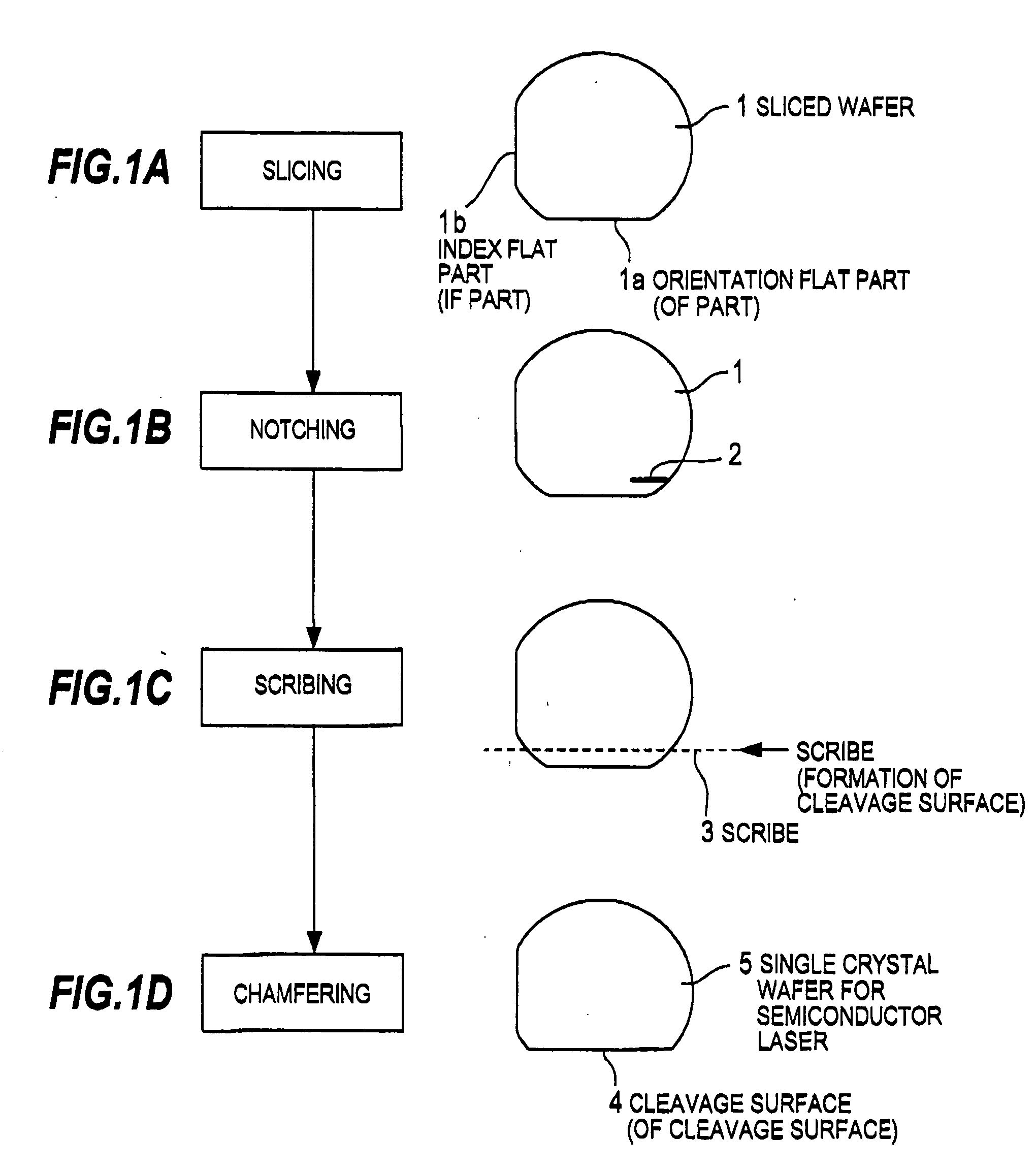
[0001] The present application is based on Japanese Patent Application No. 2005-028132 filed on Feb. 3, 2005, the entire contents of which are incorporated herein by reference. BACKGROUND OF THE INVENTION [0002] 1. Field of the Invention [0003] The present invention relates to a single crystal wafer for a semiconductor laser, and more particularly, to a single crystal wafer for a semiconductor laser with an optimized cross section of a ridge of a cleavage surface composing an orientation flat. [0004] 2. Description of the Related Art [0005] A semiconductor wafer has been used as a substrate for devices such as shot key gate field-effect transistor (MESFET), high mobility transistor (HEMT), hetero-junction bipolar transistor (HBT), laser diode (LD), and light emitting diode (LED), etc.. An active layer of such devices is formed on a surface of a mirror surface wafer fabricated from a semiconductor wafer, by using Molecular Beam Epitaxy (MBE), MetalOrganic Vapor Phase Epitaxial Growth...

Claims


Application Information

Patent Timeline
IPC IPC(8): H01L21/00H01L33/00H01L31/12H01L21/02H01L21/304H01S5/30
CPCC30B33/00H01S5/0201H01S5/02
Inventor ITANI, KENYA
Owner HITACHI CABLE
Learn More