Electronic device, semiconductor device and manufacturing method thereof

a technology of semiconductor devices and electronic devices, applied in the field of semiconductor devices, can solve the problems of increasing the waste of liquid or losing a material solution, and achieve the effect of reducing the pattern size of the semiconductor layer

Inactive Publication Date: 2006-08-03
SEMICON ENERGY LAB CO LTD
View PDF81 Cites 111 Cited by
  • Summary
  • Abstract
  • Description
  • Claims
  • Application Information

AI Technical Summary

Benefits of technology

[0012] According to the present invention, processes such as a light-exposure step or a development step can be shortened in a process for forming a conductive pattern (such as a source wiring or a drain wiring), the use amount of materials can also be reduced, and thus, costs can be largely reduced. Thus, the present invention can deal with large size substrates.
[0017] In a case of forming a wiring pattern by a droplet-discharging method, a material solution of a conductive film may be discharged intermittently from a nozzle one droplet by one droplet in the form of a dot, or a material solution of a conductive film may be discharged continuously such that droplets attached in a linear form. In the present invention, a wiring pattern may be appropriately formed by discharging the material solution of a conductive film either in the form of a dot or in the linear form. In a case of forming a wiring pattern having a relatively wide width, it leads to better productivity that the wiring pattern is formed by continuously discharging a material solution from a nozzle such that the material solution is attached in a linear form.
[0023] In a case that a material solution of a conductive film has a flow property or the flow property is increased in baking, when forming a wiring using a material solution of a conductive film by a droplet-discharging method, there is a risk that it becomes difficult to form a microscopic pattern due to the drippings of droplets. In a case that a space between wirings is narrow, there is a risk that patterns are in contact with each other. According to the present invention, a microscopic pattern can be obtained by mixing a photosensitive material into the material solution of a conductive film, precisely exposing it laser light and developing it, even if a pattern becomes wide due to the drippings of droplets.
[0029] One feature of the present invention is that a conductive layer (a source wiring or a drain wiring) formed by a droplet-discharging method is a material containing resin. This resin is a material serving as a binder or the like included in droplets including a conductive material, and this resin, a solvent and metal nano particles are mixed, so that discharging droplets by an ink-jet method becomes possible.
[0031] In each of the above structures, the drain wiring has a meandering portion, and the contact with the upper electrode is made in the meandering portion. Since the drain wiring is formed by scanning laser light, one-stroke pattern is preferable, and the conductive pattern in a portion in which a contact hole is formed, is selectively made meandering. In addition, just after forming the contact hole, the serpentine conductive film pattern and the surface of the insulating film which is not overlapped with the conductive film are exposed. By making the conductive pattern meandering (zigzag) in the contact portion, concavities and convexities are formed, and the adhesion with the upper electrode to be formed thereon can be enhanced.
[0037] The source wiring and the drain wiring electrically connect with the semiconductor layer by crossing them over the semiconductor layer, and the pattern size of the semiconductor layer can be reduced.

Problems solved by technology

When the substrate size is further increased in the future, the film formation method using spin coating has disadvantages in mass production, since a mechanism for rotating a large substrate becomes large or the loss of a material solution or waste of liquid becomes increased.

Method used


Image

  • Electronic device, semiconductor device and manufacturing method thereof
  • Electronic device, semiconductor device and manufacturing method thereof
  • Electronic device, semiconductor device and manufacturing method thereof

Examples


embodiment mode 1

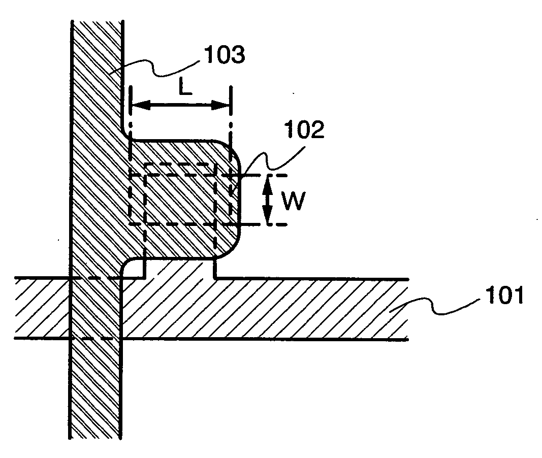
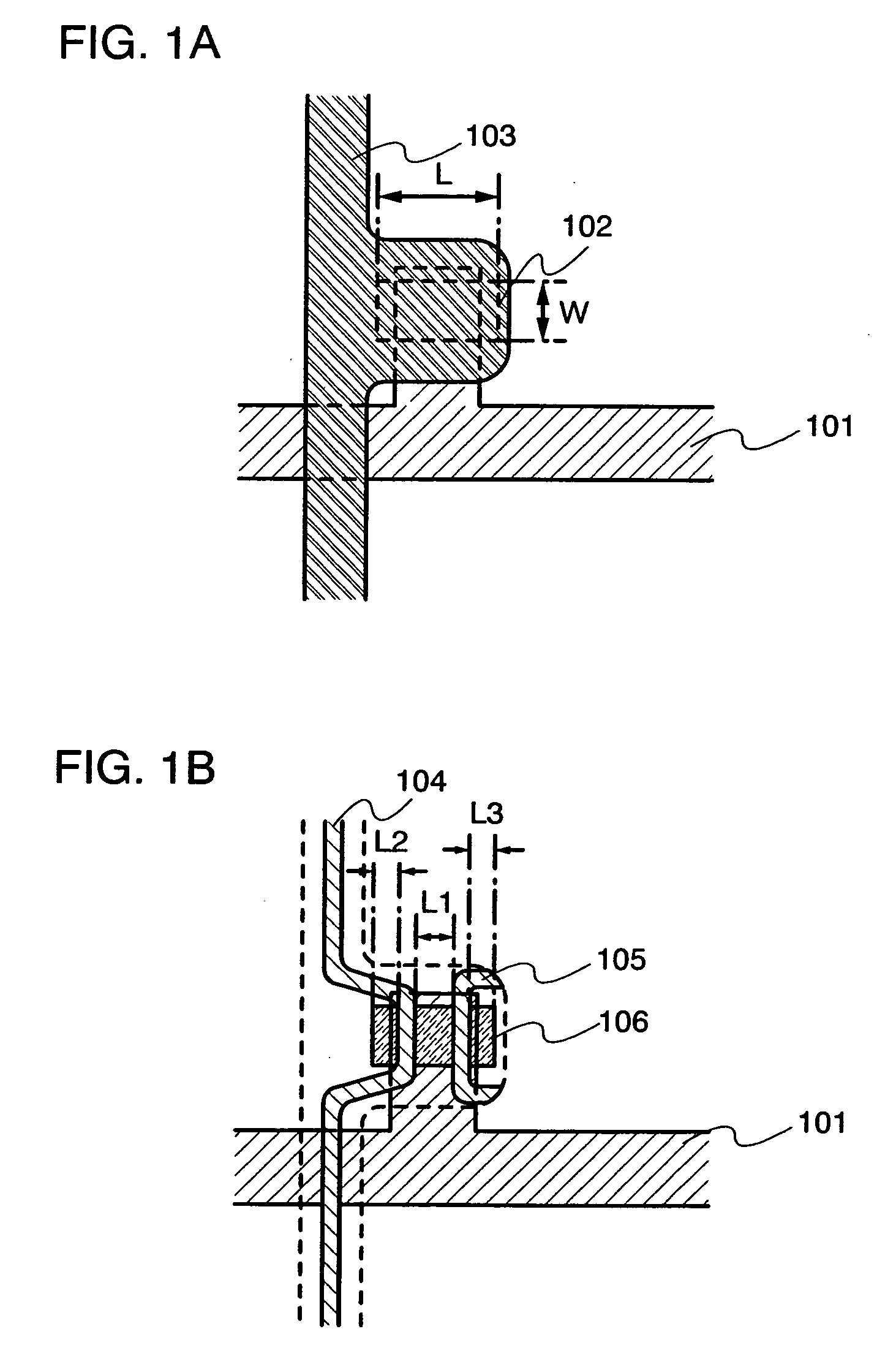
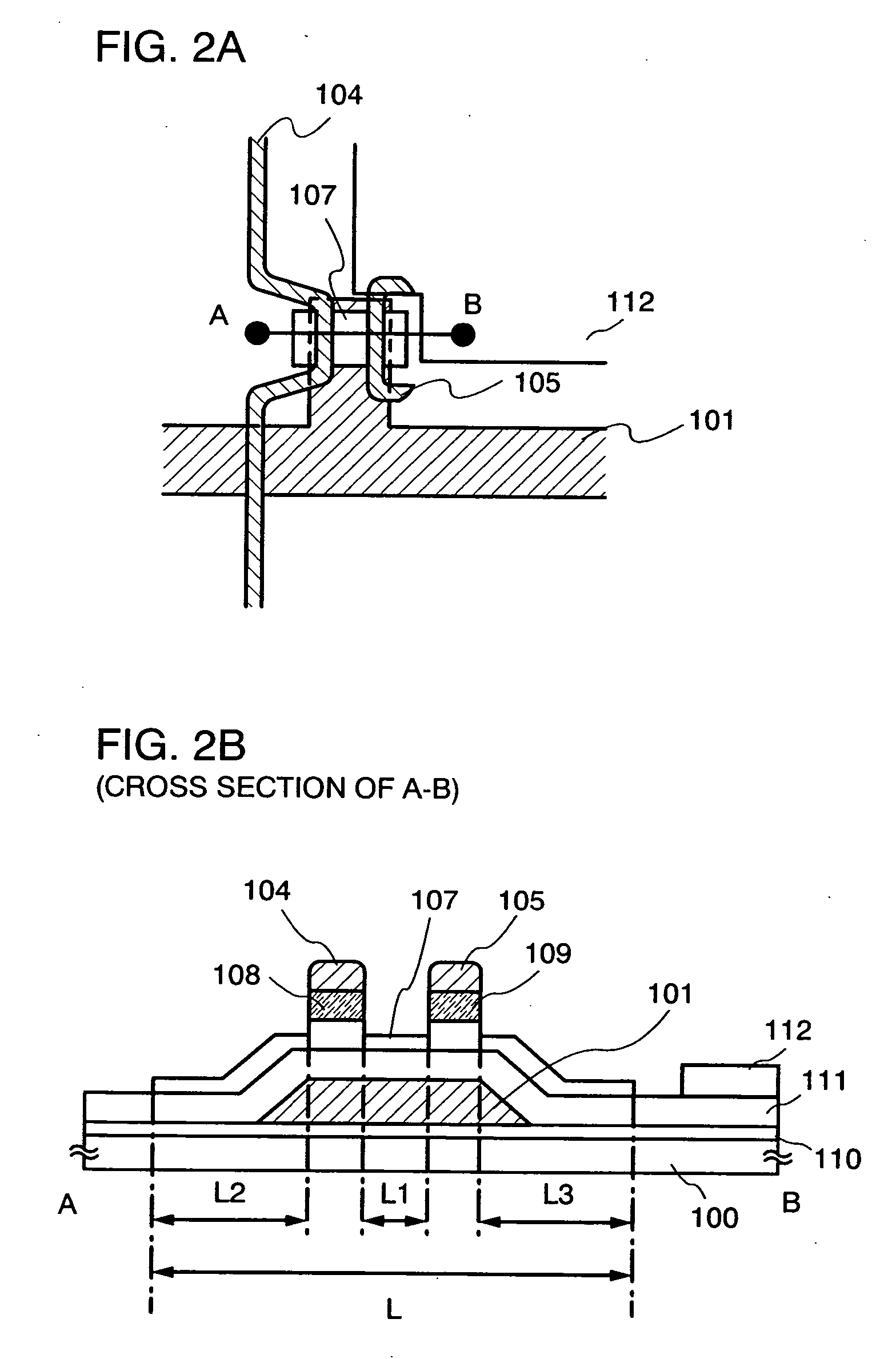
[0051] Here, a manufacturing example of an active matrix type display device using a channel-etch type TFT as a switching element, is shown in FIGS. 1A, 1B, 2A and 2B.

[0052] A base insulating film 110 is formed over a substrate 110 having an insulating surface. A base film made of an insulating film such as silicon oxide, silicon nitride, silicon oxynitride, or silicon nitride oxide is formed as the base insulating film 110. If it is not necessary, there is no particular need to form the base insulating film.

[0053] In addition to a non-alkaline glass substrate such as barium borosilicate glass, alumino borosilicate glass, or aluminosilicate glass manufactured by a fusion method or a floating method, a plastic substrate having a heat resistance that can withstand a processing temperature in this manufacturing process, or the like can be used for the substrate 100.

[0054] Thereafter, a conductive film having a thickness of 100 to 600 nm is formed by a sputtering method over the base...

embodiment mode 2

[0087] An example of manufacturing an active matrix display device having a channel-stop type TFT as a switching element with reference to FIGS. 4A, 4B, 5A and 5B.

[0088] As in Embodiment Mode 1, a base insulating film 510 is formed over a substrate 500 having an insulating surface. A base film made of an insulating film such as silicon oxide, silicon nitride, silicon nitride oxide or silicon oxynitride is formed as the base insulating film 510. If it is not necessary, there is no particular need to form the base insulating film.

[0089] Thereafter, a conductive film having a thickness of 100 to 600 nm is formed by a sputtering method over the base insulating film 510. The conductive film may be formed with a single layer of an element selected from Ta, W, Ti, Mo, Al or Cu, or an alloy material or a compound material mainly containing such an element, or a stacked layer thereof. In addition, a semiconductor film typified by a polycrystalline silicon film doped with an impurity elemen...

example 1

[0116] An active matrix type liquid crystal display device can be manufactured using a TFT shown in Embodiment Mode 1 or Embodiment Mode 2 as a switching element.

[0117] A manufacturing method of an active matrix liquid crystal display device using a TFT shown in Embodiment Mode 2 as a switching element is shown hereinafter. FIG. 6 shows an example of an active matrix liquid crystal display device. Note that similar portions in FIG. 6 to those in Embodiment Mode 2 are represented by the same reference numerals as those in Embodiment Mode 2.

[0118] An insulating film 513 is formed after forming the source wiring 504 and the drain wiring 505. A contact hole is formed in the insulating film 513 and an electrode 512 serving as a pixel electrode is formed. A transparent conductive film is used for the electrode 512.

[0119] Then, an orientation film 530 is formed to cover the electrode 512. A droplet-discharging method, a screen printing method or an offset printing method may be adopted ...


PUM


Abstract

The present invention provides a manufacturing process using a droplet-discharging method that is suitable for manufacturing a large substrate in mass production. A photosensitive material solution of a conductive film is selectively discharged by a droplet-discharging method, selectively exposed to laser light, and developed or etched, thereby allowing only the region exposed to laser light to be left and realizing a source wiring and a drain wiring having a more microscopic pattern than the pattern itself formed by discharging. One feature of the source wiring and the drain wiring is that the source wiring and the drain wiring cross an island-like semiconductor layer and overlap it.

Description

BACKGROUND OF THE INVENTION [0001] 1. Field of the Invention [0002] The present invention relates to semiconductor devices having a circuit constituted by a thin film transistor (hereinafter, also referred to as a TFT), and a manufacturing method of the semiconductor devices. For example, the present invention relates to electronic devices mounting, a part thereof, an electro-optical device typified by a liquid crystal display panel or a light-emitting display device having an organic light-emitting element. [0003] Note that a semiconductor device in this specification indicates a general device which can function with use of semiconductor characteristics, and the category of the semiconductor devices in this specification includes all types of devices such as electro-optical devices, semiconductor circuits and electronic devices. [0004] 2. Description of the Related Art [0005] In recent years, a technique for forming a thin film transistor (TFT) using a thin semiconductor film (the...

Claims


Application Information

Patent Timeline
Patent Type & Authority Applications(United States)
IPC IPC(8): H01L29/76H05B44/00
CPCH01L29/41733H01L29/458H01L29/7869H01L29/78678H01L29/66765H01L29/78696H01L27/1225G02F1/1368H01L27/1248H01L29/45H01L29/66742H01L29/78636H01L27/1218
Inventor MAEKAWA, SHINJIKUWABARA, HIDEAKI
Owner SEMICON ENERGY LAB CO LTD
Why Eureka
Try Eureka