Small-sized on-chip CMOS power amplifier having improved efficiency

a power amplifier and small chip technology, applied in the field of radio frequency (rf) system, can solve the problems of power efficiency reduction, cmos technique not stabilized, cmos on-chip not achieved, etc., and achieve the effect of maximizing output, improving efficiency, and enhancing a k factor

Active Publication Date: 2006-08-03
SAMSUNG ELECTRONICS CO LTD
View PDF8 Cites 31 Cited by
  • Summary
  • Abstract
  • Description
  • Claims
  • Application Information

AI Technical Summary

Benefits of technology

[0017] An object of the present invention is to provide a power amplifier capable of improving efficiency and maximizing output thereof by enhancing a K factor, which may cause a problem in a power amplifier having a distributed active transformer structure.
[0018] To accomplish the above and other objects, there is provided an on-chip complementary metal-oxide semiconductor (CMOS) power amplifier having an improved efficiency and being fabricated in a small size. The on-chip CMOS power amplifier includes a primary winding located at a first layer, secondary windings located at a second layer, which is an upper part of the first layer, the secondary windings being located corresponding to a position of the primary winding, and a cross section for coupling the second windings with each other.

Problems solved by technology

In particular, although the CMOS technique may be determined as an ultimate technique in which all logical circuits and all high-frequency RF analog circuits can be realized on one chip at a low price, the CMOS technique is not stabilized due to a noise characteristic in high frequencies exceeding 1 GHz and parasitic signals between parts of the CMOS.
More specifically, in the integration through the CMOS technique, CMOS on-chip is not achieved by using group III or IV compounds because power efficiency is reduced due to a low drain-gate, drain-source, or drain-substrate breakdown voltage of a CMOS and a low resistivity of a substrate.
Although the power amplifier illustrated in FIG. 1 has a simple structure, it is difficult to realize an “on-chip structure” using one chip due to the use of lumped elements.
In addition, although the power amplifier is realized as the “on-chip” according to a CMOS technique, it is difficult to solve a problem of loss due to a substrate.
Because transistors are concentrated on one spot, high temperature heat is generated, degrading the reliability of the power amplifier.
Although the power amplifier illustrated in FIG. 1 can be realized in an on-chip inductor structure, remarkable power consumption occurs due to a low substrate resistivity and a serious metal ohmic loss of the power amplifier.
In addition, a great amount of heat occurs because transistors are concentrated on one spot, and a problem of a break down voltage may occur because a great drain voltage is applied to all transistors.
However, even this amplifier causes power consumption due to passive components.
However, the power amplifier illustrated in FIG. 4 degrades the efficiency thereof because a K factor (coupling coefficient) has a value within the range of 0.5 to 06.
In addition, the power amplifier illustrated in FIG. 4 has a current crowding effect and generates an unbalanced input signal due to input feed line coupling, thereby causing serious performance degradation.

Method used


Image

  • Small-sized on-chip CMOS power amplifier having improved efficiency
  • Small-sized on-chip CMOS power amplifier having improved efficiency
  • Small-sized on-chip CMOS power amplifier having improved efficiency

Examples


Embodiment Construction

[0037] Hereinafter, preferred embodiments of the present invention will be described in detail with reference to the accompanying drawings. It is noted that the same or similar components in drawings are designated by the same reference numerals as far as possible although they are shown in different drawings. Additionally, in the following description of the present invention, a detailed description of known functions and configurations incorporated herein will be omitted when it may make the subject matter of the present invention rather unclear.

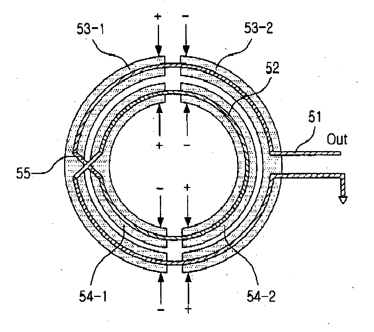
[0038]FIGS. 5A to 5C are views illustrating an on-chip CMOS power amplifier having an improved efficiency in a small size according to an embodiment of the present invention. More specifically, FIGS. 5A to 5C illustrate an on-chip CMOS power amplifier having an improved efficiency in a small size where an optimized Q transformer is easily realized and a primary winding and a secondary winding are placed on an upper layer and a lower layer...


PUM


Abstract

A small-sized on-chip complementary metal-oxide semiconductor (CMOS) Power Amplifier having improved efficiency is provided herein. The on-chip CMOS power amplifier is capable of improving efficiency and maximizing output thereof by enhancing a K factor, which may cause a problem in a power amplifier having a distributed active transformer structure. The on-chip CMOS power amplifier having an improved efficiency and being fabricated in a small size, the on-chip CMOS power amplifier includes a primary winding located at a first layer, secondary windings located at a second layer, which is an upper part of the first layer, the secondary windings being located corresponding to a position of the primary winding, and a cross section for coupling the second windings with each other.

Description

PRIORITY [0001] This application claims priority to applications entitled “Small-Sized On-Chip CMOS Power Amplifier Having Improved Efficiency” filed in the Korean Intellectual Property Office on Dec. 31, 2004 and Mar. 29, 2005 and assigned Serial No. 2004-118337 and 2005-26142, respectively, the contents of which are incorporated herein by reference. BACKGROUND OF THE INVENTION [0002] 1. Field of the Invention [0003] The present invention relates generally to a radio frequency (RF) system, and more particularly to the integration of a power amplifier section used for an RF system. [0004] 2. Description of the Related Art [0005] Recently, the trend of a radio frequency (RF) system is being focused on “RF system on-chip”. Accordingly, a monolithic microwave integrated circuit (MMIC) technique and a complementary metal oxide semiconductor (CMOS) technique are attracting attention. The MMIC technique enables that passive components such as resistors, inductors, and capacitors and activ...

Claims


Application Information

Patent Timeline
Patent Type & Authority Applications(United States)
IPC IPC(8): H03F3/14
CPCH03F1/02H03F1/22H03F3/195H03F3/265H03F3/604H03F2200/537H03F2200/541
Inventor LEE, JAE-SUPKANG, HYUN-ILLEE, SEONG-SOOLOTHAR, HOLGERKO, JU-HYUNBAEK, DONG-HYUNHONG, SONG-CHEOL
Owner SAMSUNG ELECTRONICS CO LTD
Why Eureka
Try Eureka