Method of forming gate dielectric layer

a dielectric layer and gate technology, applied in the direction of semiconductor devices, basic electric elements, electrical equipment, etc., can solve the problems of reducing the tunneling effect of electrons, reducing the leakage current of devices miniaturized, etc., and achieving the effect of reducing the tunneling curren

Active Publication Date: 2006-08-03
UNITED MICROELECTRONICS CORP
View PDF5 Cites 13 Cited by
  • Summary
  • Abstract
  • Description
  • Claims
  • Application Information

AI Technical Summary

Benefits of technology

[0008] Accordingly, one objective of the present invention is to provide a method of forming a gate dielectric layer capable of reducing tunneling current and solving other related problems.

Problems solved by technology

The reason is that the shallow nitrogen distribution formed by the conventional process still causes a higher leakage current when the device is miniaturized.
The gate dielectric layer having a shallow nitrogen distribution can only suppress the electron tunneling effect to a limited extent.

Method used


Image

  • Method of forming gate dielectric layer
  • Method of forming gate dielectric layer
  • Method of forming gate dielectric layer

Examples


Embodiment Construction

[0021] Reference will now be made in detail to the present embodiments of the invention, examples of which are illustrated in the accompanying drawings. Wherever possible, the same reference numbers are used in the drawings and the description to refer to the same or like parts.

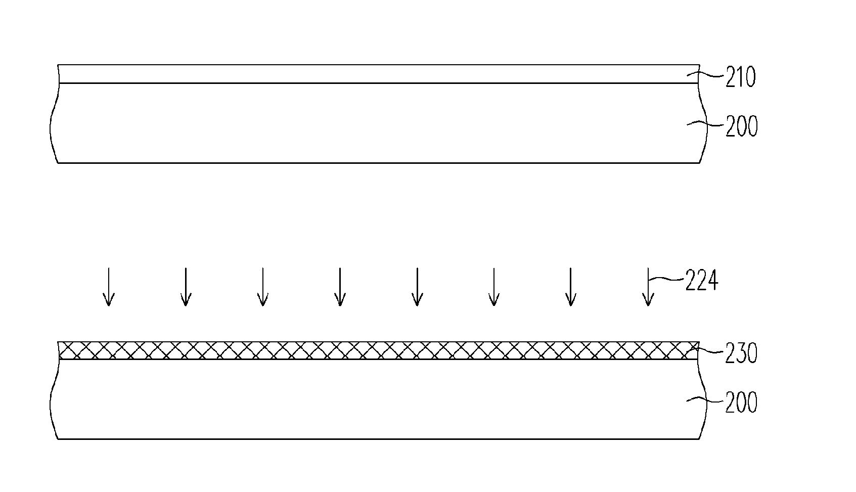
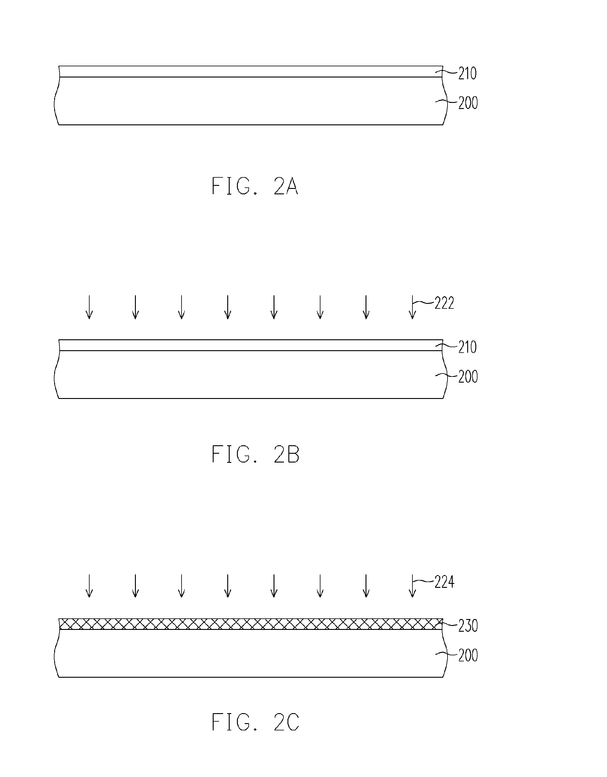
[0022]FIGS. 2A through 2C are schematic cross-sectional views showing the steps for forming a gate dielectric layer according to one embodiment of the present invention. As shown in FIG. 2A, a silicon oxide layer 210 is formed on a semiconductor substrate 200. The silicon oxide layer 210 is formed with, for example, thermal oxidation or chemical vapor deposition (CVD). Thereafter, as shown in FIGS. 2B and 2C, a first nitrogen doping process 222 and a second nitrogen doping process 224 are performed to the silicon oxide layer 210 using a plasma containing inert gas (for example, helium) and gaseous nitrogen to form a gate dielectric layer 230. In the embodiment of the present invention, the first nitrogen dop...


PUM


Abstract

A method for forming a gate dielectric layer is described. A silicon oxide layer is formed on a semiconductor substrate. Then, a first and a second nitrogen doping processes are performed in sequence to the silicon oxide layer using plasma comprising inert gas and gaseous nitrogen to form a gate dielectric layer. The first nitrogen doping process is performed at a lower power, a lower pressure and a higher inert gas to nitrogen gas ratio than those at the second nitrogen doping process. The combination of the deeper nitrogen distribution of the first nitrogen doping process and the shallower nitrogen distribution of the second nitrogen doping process produces a flatter total nitrogen distribution profile so that leakage current from electron tunneling through the gate dielectric layer can be reduced.

Description

BACKGROUND OF THE INVENTION [0001] 1. Field of the Invention [0002] The present invention relates to a semiconductor device manufacturing method. More particularly, the present invention relates to a method of forming a gate dielectric layer. [0003] 2. Description of the Related Art [0004] With the trend of more miniaturized metal-oxide-semiconductor (MOS) devices, the quality of a gate dielectric layer is highly required. For example, the leakage current must be as low as possible. When the gate dielectric layer is made of silicon oxide, most manufacturers will perform a nitrogen doping process to adjust the quality of the gate dielectric layer and minimize leakage. To prevent possible impact on the threshold voltage, the flatband voltage between the substrate and the gate and the reliability of the device, a shallow nitrogen distribution is preferred in the nitrogen doping process. [0005] However, to minimize the leakage current of the device, a flatter nitrogen distribution curve...

Claims


Application Information

Patent Timeline
Patent Type & Authority Applications(United States)
IPC IPC(8): H01L21/00H01L21/31H01L21/469
CPCH01L21/28202H01L21/3144H01L29/518H01L21/0214H01L21/0234H01L21/02332
Inventor WANG, YU-RENYEN, YING-WEICHENG, LIYUANHUANG, KUO-TAI
Owner UNITED MICROELECTRONICS CORP
Why Eureka
Try Eureka