Post etch copper cleaning using dry plasma

a technology of dry plasma and etching copper, which is applied in the direction of semiconductor/solid-state device manufacturing, basic electric elements, electric apparatus, etc., can solve the problems of forming contaminants, oxidation of exposed copper surfaces, and undesirable contaminants

Inactive Publication Date: 2006-08-10
TAIWAN SEMICON MFG CO LTD
View PDF3 Cites 196 Cited by
  • Summary
  • Abstract
  • Description
  • Claims
  • Application Information

AI Technical Summary

Problems solved by technology

A shortcoming associated with the use of copper interconnect technology is that the exposed copper surfaces are prone to oxidation.
The materials conventionally used to passivate the copper surface after polishing, however, may complex with species used in the formation of further materials over the passivated copper surface, to form undesirable contaminants.
When the optional etch stop layer is not used, contaminants may be formed during the initial stages of the further dielectric deposition.
Applicants have noted that, regardless of the condition of the copper surface prior to the formation of the subsequent film such as the optional etch-stop film and/or the overlying dielect

Method used


Image

  • Post etch copper cleaning using dry plasma
  • Post etch copper cleaning using dry plasma
  • Post etch copper cleaning using dry plasma

Examples


Embodiment Construction

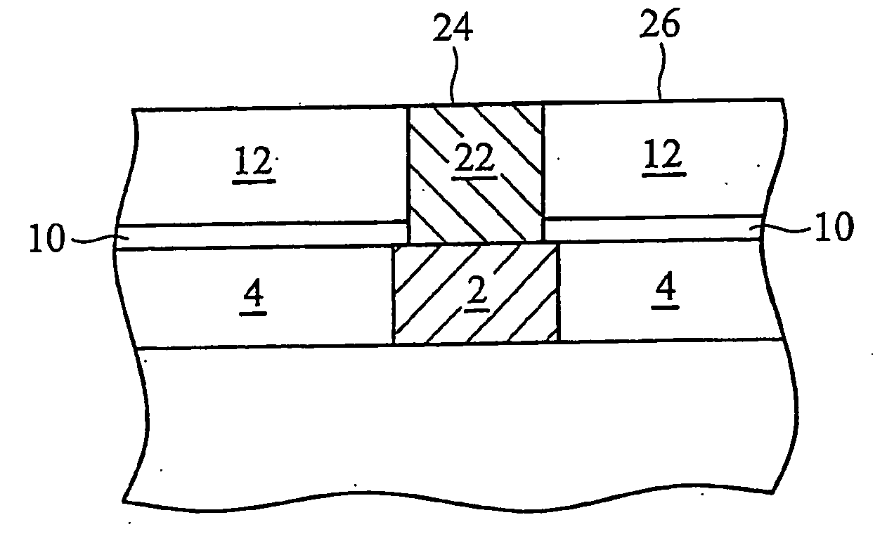
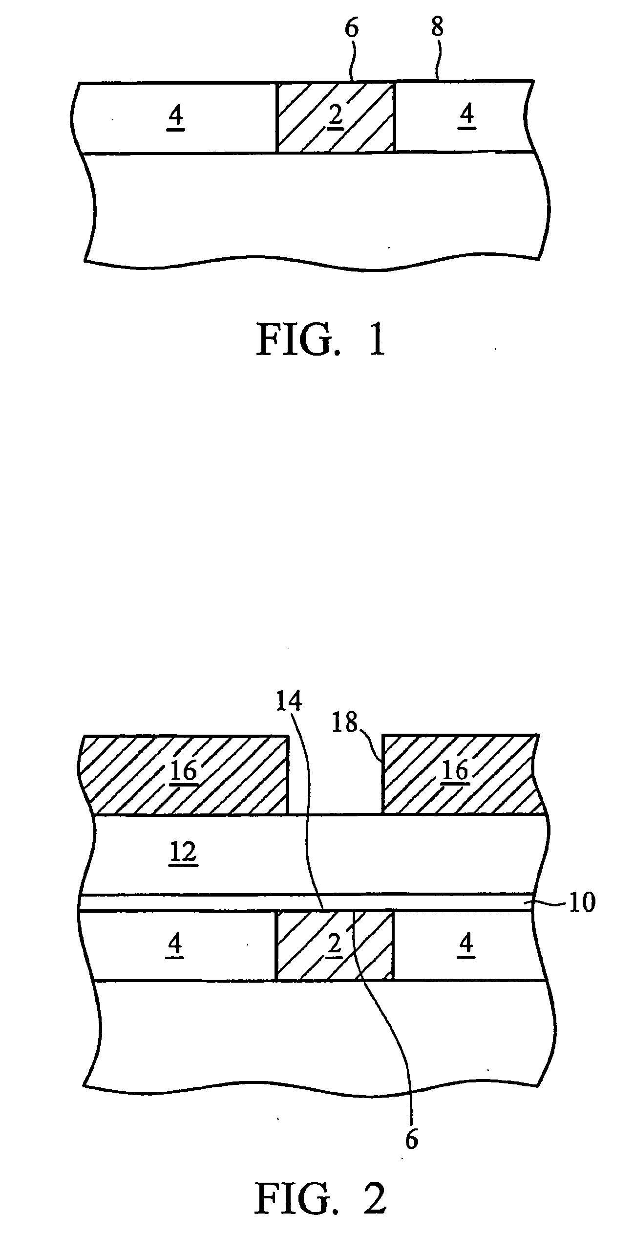
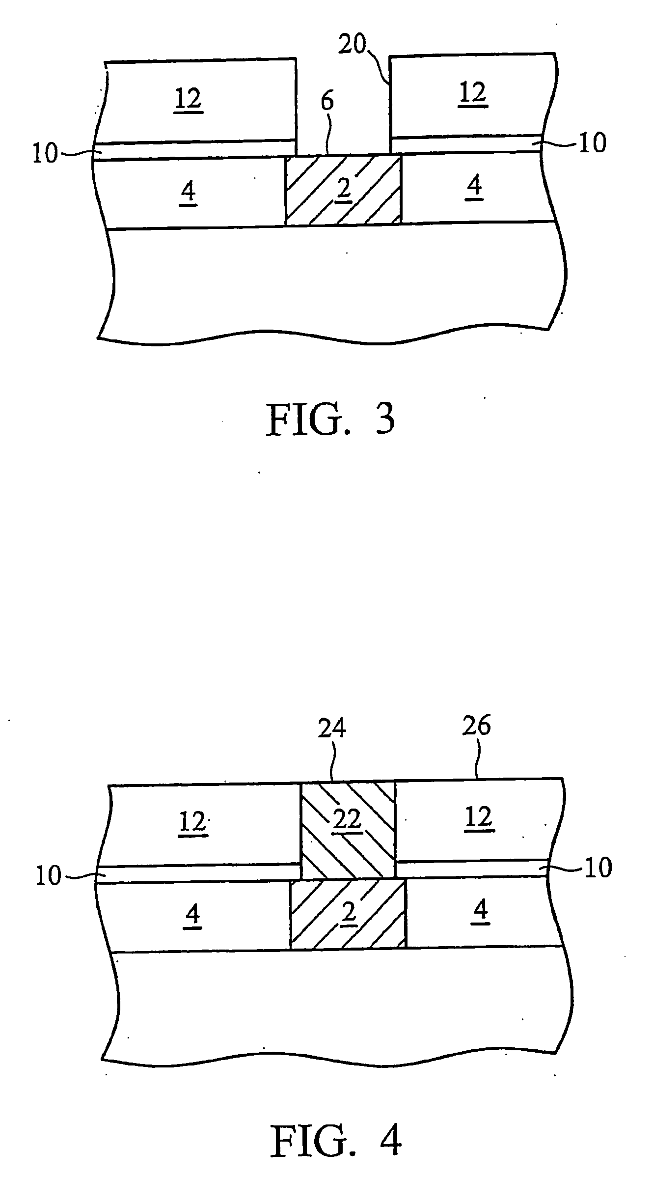
[0013]FIG. 1 is a cross-sectional view showing copper structure 2 inlaid within dielectric 4 according to damascene processing technology. A polishing operation such as chemical mechanical polishing may be used to form the structure which includes top surface 6 of copper structure 2 and top surface 8 of dielectric 4 which are substantially co-planar. Dielectric 4 may be any of various suitable dielectrics used in semiconductor manufacturing, including low-k dielectric materials and various oxides and oxynitrides. After the structure shown in FIG. 1 is formed, top surface 6 of copper structure 2 may be passivated using conventional techniques. According to one exemplary embodiment, the passivation process may include treating with an anti-corrosion solvent such as BTA (Benzotriazole) using conventional methods, but other anti-corrosion solvents and other passivation techniques may be used in other exemplary embodiments. In still further exemplary embodiments, the passivation techniqu...


PUM


Abstract

A method for post-etch copper cleaning uses a hydrogen plasma with a trace gas additive constituting about 3-10 percent of the plasma by volume to clean a copper surface exposed by etching. The trace gas may be atomic nitrogen or other species having an atomic mass of 15 or greater. The trace gas adds a sputtering aspect to the plasma cleaning and removes polymeric etch by-products and polymeric and other residuals formed during the deposition of dielectric materials or etch stop layers over the copper surface. An anti-corrosion solvent may be used to passivate the copper surface prior to formation of the dielectric materials or etch stop layers.

Description

FIELD OF THE INVENTION [0001] The present invention relates most generally to semiconductor devices and methods for their fabrication. More particularly, the present invention is directed to a cleaning method and structure that provide copper contact structures with low contact resistance. BACKGROUND [0002] The use of copper as a conductive interconnect material is favored in semiconductor devices because of the high speed that copper provides. Copper is difficult to pattern and therefore copper interconnect leads are typically formed using damascene processing technology whereby an opening is formed in a dielectric, copper is deposited over the dielectric and within the opening, then a polishing / planarization process is used to remove copper from over the dielectric, leaving the copper inlaid within the opening. The inlaid copper includes an upper surface that is essentially co-planar with the top surface of the dielectric in which the copper is disposed. A shortcoming associated w...

Claims


Application Information

Patent Timeline
IPC IPC(8): H01L21/44
CPCH01L21/02063H01L21/321H01L21/76802H01L21/76814
Inventor YEH, CHEN-NANHSU, MIAO-JUTAO, HUN-JAN
Owner TAIWAN SEMICON MFG CO LTD
Why Eureka
Try Eureka