Semiconductor device, method of manufacturing the same, capacitor structure, and method of manufacturing the same

a semiconductor device and capacitor technology, applied in the direction of semiconductor/solid-state device details, semiconductor devices, electrical apparatus, etc., can solve the problems of increasing the manufacturing cost of the semiconductor device, difficult to meet the requirement of multi-layer ceramic capacitors, and difficult to reduce inductance, so as to reduce the interconnection line length, reduce the impedance, and reduce the inductance

Inactive Publication Date: 2006-08-17
FUJITSU LTD
View PDF3 Cites 61 Cited by
  • Summary
  • Abstract
  • Description
  • Claims
  • Application Information

AI Technical Summary

Benefits of technology

[0035] According to one aspect of the present invention, a first pad electrode is electrically connected to the odd-numbered ones of electrodes from the substrate side, and a second pad electrode is electrically connected to the even-numbered one or more of the electrodes from the substrate side, thereby connecting multiple capacitors of the substantially same capacitance in parallel between the first pad electrode and the second pad electrode. Accordingly, it is possible to achieve a capacitor structure of reduced impedance by reducing inductance by reducing interconnection line length required in configuring a decoupling capacitor.

Problems solved by technology

A large capacitance can be provided, but it is not easy to reduce inductance because the electrode layers are connected to the surface electrodes on the side surfaces.
However, it is difficult to meet this requirement with multilayer ceramic capacitors.
In order to form these through holes 504, it is necessary to use ICP (Induction Coupling Plasma), which causes the problem of an increasing manufacturing cost of the semiconductor device 500.
This causes a problem in that the decoupling capacitors 505 are likely to be poorly isolated, thus resulting in a reduced yield.
However, this results in the problem of higher costs because electrodes and a dielectric film are formed and patterned for each layer.
Further, since the thin film capacitor is formed on a patterned uneven underlayer, there is a problem in that a poor yield rate due to unevenness of the film thickness of a dielectric film and to dust causes an increase in costs.

Method used


Image

  • Semiconductor device, method of manufacturing the same, capacitor structure, and method of manufacturing the same
  • Semiconductor device, method of manufacturing the same, capacitor structure, and method of manufacturing the same
  • Semiconductor device, method of manufacturing the same, capacitor structure, and method of manufacturing the same

Examples


first embodiment

[0078] [First Embodiment]

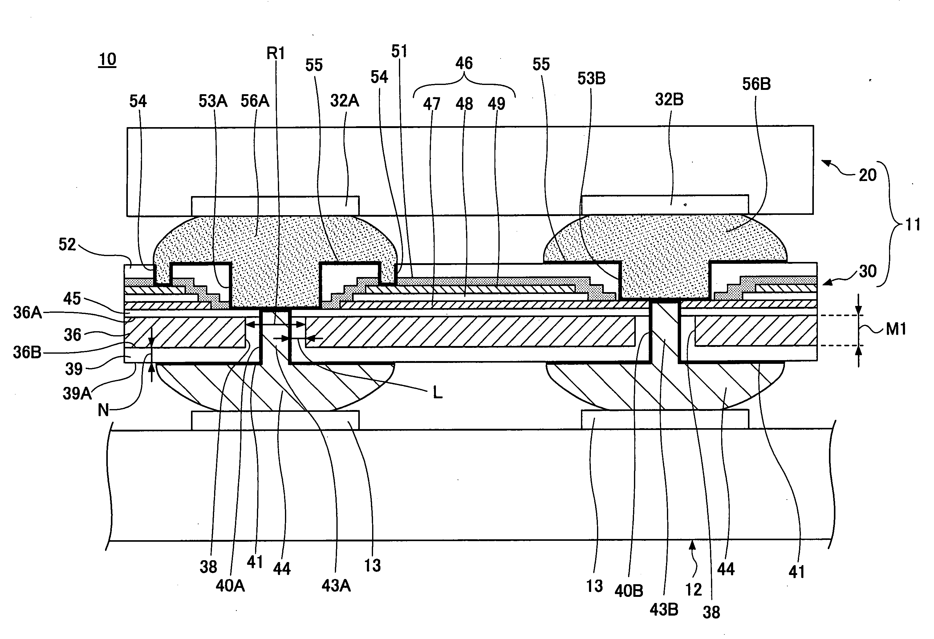
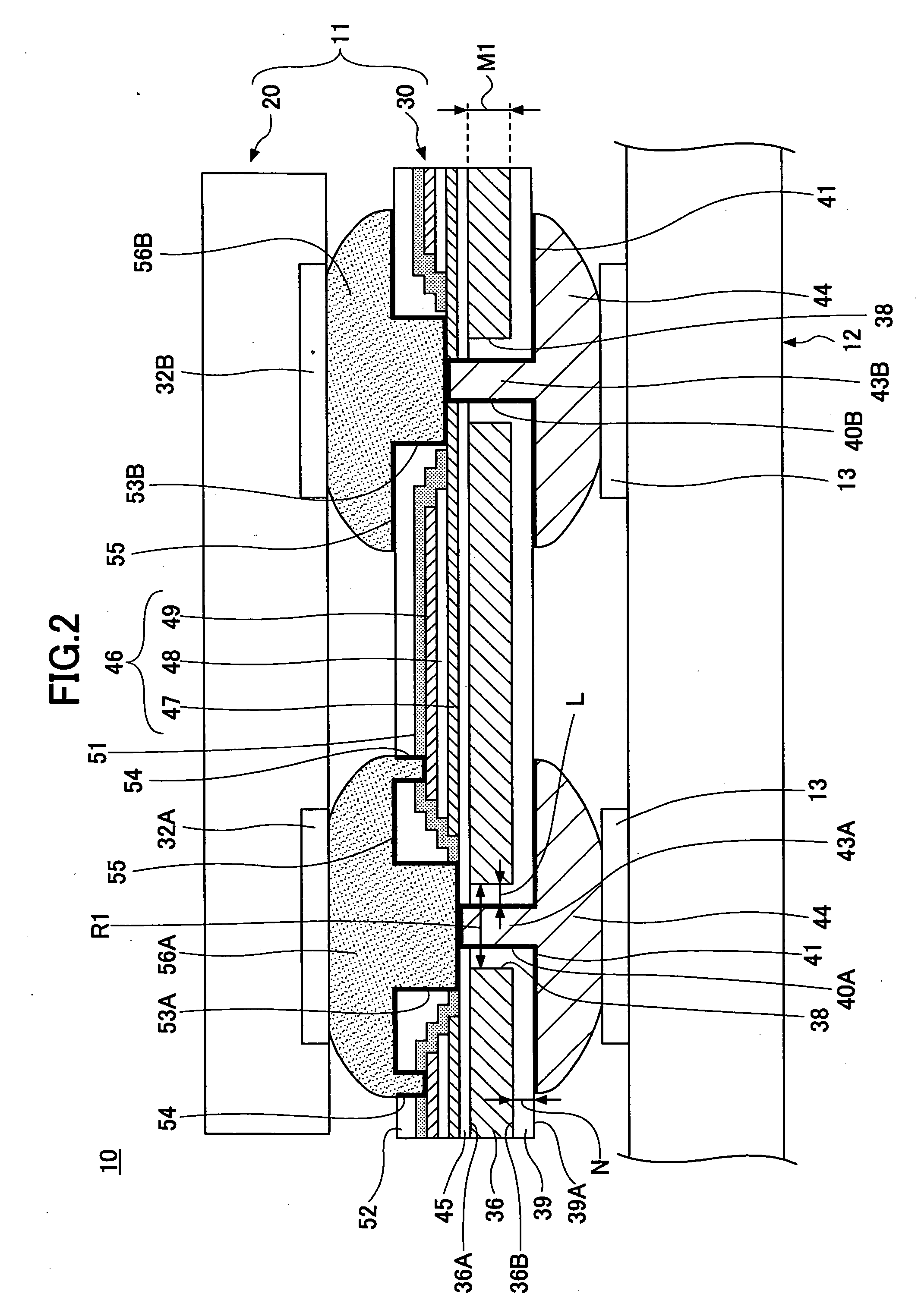
[0079]FIG. 2 is a cross-sectional view of an electronic device 10 according to a first embodiment of the present invention.

[0080] Referring to FIG. 2, the electronic device according to this embodiment includes a semiconductor device 11 and a circuit board 12 on which the semiconductor device 11 is mounted. Multiple external connection terminals 44 of the semiconductor device 11 are electrically connected to corresponding connection pads 13 provided on the circuit board 12.

[0081] The semiconductor device 11 includes a semiconductor chip 20 and an interposer 30. The semiconductor chip 20 includes at least one connection pad 32A and at least one connection pad 32B. The connection pad 32A, which is an electrode pad for power supply (a power supply electrode pad), is connected to a corresponding internal connection terminal 56A provided on the first main surface side of the interposer 30. The connection pad 32B, which is an electrode pad for ground (a ground e...

second embodiment

[0157] [Second Embodiment]

[0158]FIG. 8 is a cross-sectional view of a semiconductor device 100 according to a second embodiment of the present invention. In FIG. 8, the same elements as those of the semiconductor device 11 of the first embodiment are referred to by the same numerals, and a description thereof is omitted.

[0159] Referring to FIG. 8, the semiconductor device 100 according to this embodiment is equal in configuration to the semiconductor device 11 of the first embodiment except that a resistive element 102 that is a passive element is provided.

[0160] The resistive element 102 includes a pair of electrodes 103 and 104 and a resistor 105, and is formed on the interposer 30. The electrode 103 is formed on the insulating film 52, and is electrically connected to the internal connection terminal 56A. As a result, the electrode 103 is electrically connected to the thin film capacitor 46 and the corresponding external connection terminal 44 through the internal connection te...

third embodiment

[0164] [Third Embodiment]

[0165]FIG. 9 is a cross-sectional view of a semiconductor device 110 according to a third embodiment of the present invention. Referring to FIG. 9, the semiconductor device 110 includes a semiconductor substrate 111 on which a semiconductor circuit 112, which is an internal circuit, is formed; through vias 113 passing through the semiconductor substrate 111; and external connection terminals 114 and 115 formed at corresponding ends of each through via 113. The semiconductor circuit 112 may include an active element.

[0166] The semiconductor substrate 111 is a thinned plate. The thickness M2 of the semiconductor substrate 111 is the same value as the thickness M1 of the Si substrate 36 described in the first embodiment.

[0167] The semiconductor circuit 112 is electrically connected to the through vias 113. The through vias 113 are formed by the same method as the through vias 43A and 43B described in the first embodiment (FIGS. 3H through 3K). That is, the th...


PUM


Abstract

A semiconductor device is disclosed that includes an interposer and a semiconductor chip. The interposer includes a Si substrate; multiple through vias provided through an insulating material in corresponding through holes passing through the Si substrate; a thin film capacitor provided on a first main surface of the Si substrate so as to be electrically connected to the through vias; and multiple external connection terminals provided on a second main surface of the Si substrate so as to be electrically connected to the through vias. The second main surface faces away from the first main surface. The semiconductor chip is provided on one of the first main surface and the second main surface so as to be electrically connected to the through vias. The Si substrate has a thickness less than the diameter of the through holes.

Description

CROSS-REFERENCE TO RELATED APPLICATION [0001] The present application is based on Japanese Priority Patent Applications No. 2005-036514, filed on Feb. 14, 2005, and No. 2005-237777, filed on Aug. 18, 2005, the entire contents of which are hereby incorporated by reference. BACKGROUND OF THE INVENTION [0002] 1. Field of the Invention [0003] The present invention relates generally to semiconductor devices, methods of manufacturing the same, capacitor structures, and methods of manufacturing the same, and more particularly to a semiconductor device having a semiconductor chip and an interposer including a capacitor and a through via, a method of manufacturing the same, a capacitor structure, and a method of manufacturing the same. [0004] 2. Description of the Related Art [0005] Electronic apparatuses are now becoming more sophisticated with more functions in the fields of personal computers, cellular phones, and other mobile equipment. [0006] In order to prevent malfunction due to switc...

Claims


Application Information

Patent Timeline
Patent Type & Authority Applications(United States)
IPC IPC(8): H01L23/48
CPCH01L21/4853H01L21/4857H01L21/6835H01L23/147H01L23/481H01L23/49816H01L23/49822H01L23/49827H01L23/50H01L23/66H01L24/16H01L24/81H01L2221/68345H01L2221/68359H01L2221/68368H01L2224/13099H01L2224/16225H01L2224/81801H01L2924/01013H01L2924/01015H01L2924/01018H01L2924/01022H01L2924/01025H01L2924/01029H01L2924/01033H01L2924/01038H01L2924/0104H01L2924/01042H01L2924/01046H01L2924/01056H01L2924/01057H01L2924/01061H01L2924/01073H01L2924/01074H01L2924/01077H01L2924/01078H01L2924/01079H01L2924/01082H01L2924/09701H01L2924/14H01L2924/15311H01L2924/19041H01L2924/19042H01L2924/19043H01L2924/19106H01L2924/30105H01L2924/30107H01L2924/3011H01L2924/01005H01L2924/01006H01L2924/01019H01L2924/01023H01L2924/01024H01L2924/01041H01L2924/01044H01L2924/01045H01L2924/01047H01L2924/0105H01L2924/01072H01L2924/014H01L2224/14051H01L2224/13018H01L2224/13022H01L2224/16235H01L2924/00012H01L2924/12042H01L2224/0557H01L2224/05573H01L2924/00014H01L2224/05571H01L2224/05096H01L2224/05091H01L2224/0554H01L2924/00H01L2224/05599H01L2224/0555H01L2224/0556H01L27/04H01L23/12H01L25/04
Inventor KURIHARA, KAZUAKISHIOGA, TAKESHIBANIECKI, JOHN D.
Owner FUJITSU LTD
Why Eureka
Try Eureka