Dummy wafer

a technology of dummy wafers and silicon chips, applied in the field of dummy wafers, can solve the problems of high cost and brittleness of silicon dummy wafers, inability to reuse, and difficult to respond to light sensors, etc., and achieve the effect of high strength and easy response to light sensors

Inactive Publication Date: 2006-08-24
NIPPON OIL CORP
View PDF11 Cites 5 Cited by
  • Summary
  • Abstract
  • Description
  • Claims
  • Application Information

AI Technical Summary

Benefits of technology

[0009] It is an object of the present invention to provide a dummy wafer that is rigid and has a high strength even when it is thin and of large diameter, e.g., 300 mm in diameter×0.5 mm to 0.75 mm in th...

Problems solved by technology

Heretofore, the following dummy wafers have been used in the process for manufacturing semiconductor devices, and each of them has had a problem: (a) Silicon dummy wafer: It is expensive and brittle, and cannot be reused.
Since the number ...

Method used


Image

  • Dummy wafer
  • Dummy wafer
  • Dummy wafer

Examples


example 1

Lamination Forming of Dummy Wafer

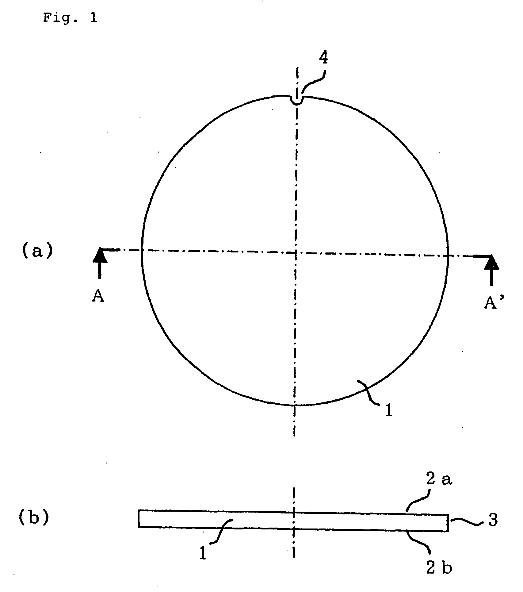
[0125] A dummy wafer shown in FIG. 4 was fabricated using the procedures described below:

(1) Manufacture of Resin Composition for Composite Material

[0126] As a bis-phenol-A epoxy resin, 30 parts by mass of Epotohto YD 128 (trade name, manufactured by Tohto Kasei Co., Ltd.), as a phenol novolak epoxy resin, 50 parts by mass of Epotohto YDPN 638 (trade name, manufactured by Tohto Kasei Co., Ltd.), and as a phenoxy resin, 10 parts by mass of Phenotohto YP 50 (trade name, manufactured by Tohto Kasei Co., Ltd.) were mixed at 200° C. for 1.5 hours, and cooled to 90° C. To this mixture, 20 parts by mass of Epotohto YH 434 (trade name, manufactured by Tohto Kasei Co., Ltd.), which is a glycidyl-amine epoxy resin, and 40 parts by mass of 4,4′-diaminodiphenyl sulfone (DDS) (trade name: Seikacure S, manufactured by Wakayama Kasei Kogyou Co. Ltd.), which is a curing agent. are evenly mixed under a vacuum degassing to obtain a heat-resistant epoxy resin compo...

example 2

(1) Structure of resin composition for composite material

[0138] An epoxy resin composition was fabricated in the same manner as in Example 1.

(2) Fabrication of Dummy Wafer

[0139] There were used three kinds of unidirectional prepreg sheets: a unidirectional prepreg sheet obtained by drawing and aligning pitch-based carbon fibers having a tensile modulus of 500 GPa in one direction and impregnating them with the epoxy resin composition obtained in the above (1) (fiber mass per unit area: 50 g / m2, resin content: 38% by mass, thickness: 0.048 mm); a unidirectional prepreg sheet obtained by drawing and aligning pitch-based carbon fibers having a tensile modulus of 800 GPa in one direction and impregnating them with the epoxy resin composition obtained in the above (1) (fiber mass per unit area: 50 g / m2, resin content: 38% by mass, thickness: 0.048 mm); and a unidirectional prepreg sheet obtained by drawing and aligning PAN-based carbon fibers having a tensile modulus of 230 GPa in o...

example 3

(1) Manufacture of Resin Composition for Composite Material

[0152] An epoxy resin composition was fabricated in the same manner as in Example 1.

(2) Fabrication of Dummy Wafer

[0153] There were used three kinds of unidirectional prepreg sheets: a unidirectional prepreg sheet obtained by drawing and aligning PAN-based carbon fibers having a tensile modulus of 230 GPa in one direction and impregnating them with the epoxy resin composition obtained in the above (1) (fiber mass per unit area: 50 g / m2, resin content: 38% by mass, thickness: 0.052 mm); a unidirectional prepreg sheet obtained by drawing and aligning PAN-based carbon fibers having a tensile modulus of 380 GPa in one direction and impregnating them with the epoxy resin composition obtained in the above (1) (fiber mass per unit area: 45 g / m2, resin content: 38% by mass, thickness: 0.047 mm); and a unidirectional prepreg sheet obtained by drawing and aligning PAN-based carbon fibers having a tensile modulus of 230 GPa in one...


PUM

PropertyMeasurementUnit
Temperatureaaaaaaaaaa
Fractionaaaaaaaaaa
Fractionaaaaaaaaaa

Abstract

A dummy wafer including a carbon fiber reinforced plastic (CFRP). Specifically the dummy wafer has a wafer substrate including CFRP, the substrate has two skin layers disposed on respective principal surface side and a core layer interposed between the skin layers, and each of the skin layers has multiple one-dimensionally reinforced layers consisting of a cured and shaped product of unidirectional prepreg. With reference to the orientation direction of one of the one-dimensionally reinforced layers on the side closest to the principal surface (outermost layer) in each of the skin layers, the other outermost layer is oriented in a specific direction; the tensile modulus of CF in each outermost layer is within a specific range; each skin layer has a one-dimensionally reinforced layer that contains CF oriented in a specific direction and has the tensile modulus within a specific range; and the core layer has a one-dimensionally reinforced layer that contains CF oriented in a specific direction and having the tensile modulus within a specific range, and a one-dimensionally reinforced layer that contains CF oriented in a specific direction and having the tensile modulus within a specific range. The dummy wafer has high strength, is inexpensive, and easily responds to light sensors.

Description

TECHNICAL FIELD [0001] The present invention relates to a dummy wafer that is used in a process for manufacturing a semiconductor such as a semiconductor integrated circuit and a semiconductor memory. BACKGROUND ART [0002] Heretofore, in processes for manufacturing semiconductors, such as semiconductor integrated circuits and semiconductor memories, processing known as dummy processing, wherein various processing is performed using a dummy wafer on which no actual IC pattern is formed, has been performed for the operation test of, for example, a plasma etching apparatus, a CVD apparatus, a sputtering apparatus or the like; the number adjustment of wafers in batch process; the countermeasure against the loading effect; or the like. In addition, when cleaning of the reaction chamber of various plasma apparatuses, such as a plasma CVD apparatus is performed with plasma cleaning, a dummy wafer has also been used for protecting a substrate-supported electrode from the plasma. [0003] Here...

Claims


Application Information

Patent Timeline
IPC IPC(8): H01L23/58C08J5/04H01L21/00
CPCC08J5/042C08J2363/00H01L21/67259H01L21/20
Inventor UCHIDA, DAISUKEKOBAYASHI, TAKASHIAOYAGI, KENICHI
Owner NIPPON OIL CORP
Why Eureka
Try Eureka