Adhesive transfer method of carbon nanotube layer

a carbon nanotube and adhesive technology, applied in the field of adhesive transfer methods of carbon nanotube layers, can solve the problems of limiting the range of potential applications, low flexibility of such electrodes, and high cost of fabrication methods

Inactive Publication Date: 2006-08-24
EASTMAN KODAK CO
View PDF12 Cites 220 Cited by
  • Summary
  • Abstract
  • Description
  • Claims
  • Application Information

AI Technical Summary

Benefits of technology

[0031] The invention provides a desirable transfer element and a transfer method to form conductive layers, especially those comprising SWCNT or SWCNT and electronically conductive polymers on receiver substrates, and incorporating such receivers in electronic and / or optical devices.

Problems solved by technology

The high cost of the fabrication methods and the low flexibility of such electrodes, due to the brittleness of the inorganic ITO layer as well as the glass substrate, limit the range of potential applications.
Thus, SWCNTs have been extremely difficult to process for various uses.
This method is disadvantaged due to the high number of steps to achieve a transferred SWCNT film which increases the probability for error and low yield.
Additionally, there is an initial flocculation step of the very dilute SWCNT dispersion, using methanol to remove the excessive surfactant in the SWCNT dispersion, which can be difficult to control and decrease yields of this process.
This method is further disadvantaged by the very low SWCNT weight percent in the starting dispersion (˜0.05 mg / mL or 50 ppm / 0.005 wt %) and a surfactant weight percent of ˜1 wt % or 10,000 ppm which can significantly decrease electronic transport in films.
The dispersion concentrations used in these methods make it very difficult to produce images via direct deposition (inkjet etc.) techniques.
Further, such high solvent loads due to the low solids dispersions create long process times and difficulties handling the excess solvent.
Such photoablation processes are convenient, dry, one-step methods but the generation of debris may require a wet cleaning step and may contaminate the optics and mechanics of the laser device.
Although there is considerable art describing various methods to form and pattern electronically conductive layers, there are some applications where it may be difficult or impractical to involve any wet processing or cumbersome patterning steps.
For example, wet processing during coating and / or patterning may adversely affect integrity, interfacial characteristics, and / or electrical or optical properties of the previously deposited layers.
Additionally, the device manufacturer may not have coating facilities to handle large quantity of liquid.
It is conceivable that many potentially advantageous device constructions, designs, layouts, and materials are impractical because of the limitations of conventional wet coating and patterning.
However, such elements are non-transparent, often including a light-to-heat conversion layer, interlayer, release layer and the like.
Construction of such multilayered elements are complex, involved and prone to defects that can get incorporated into the final device.
However, such methods are prone to creating dirt and debris that may not be tolerated for many display applications.

Method used


Image

  • Adhesive transfer method of carbon nanotube layer
  • Adhesive transfer method of carbon nanotube layer
  • Adhesive transfer method of carbon nanotube layer

Examples


examples

[0159] Donor Laminates

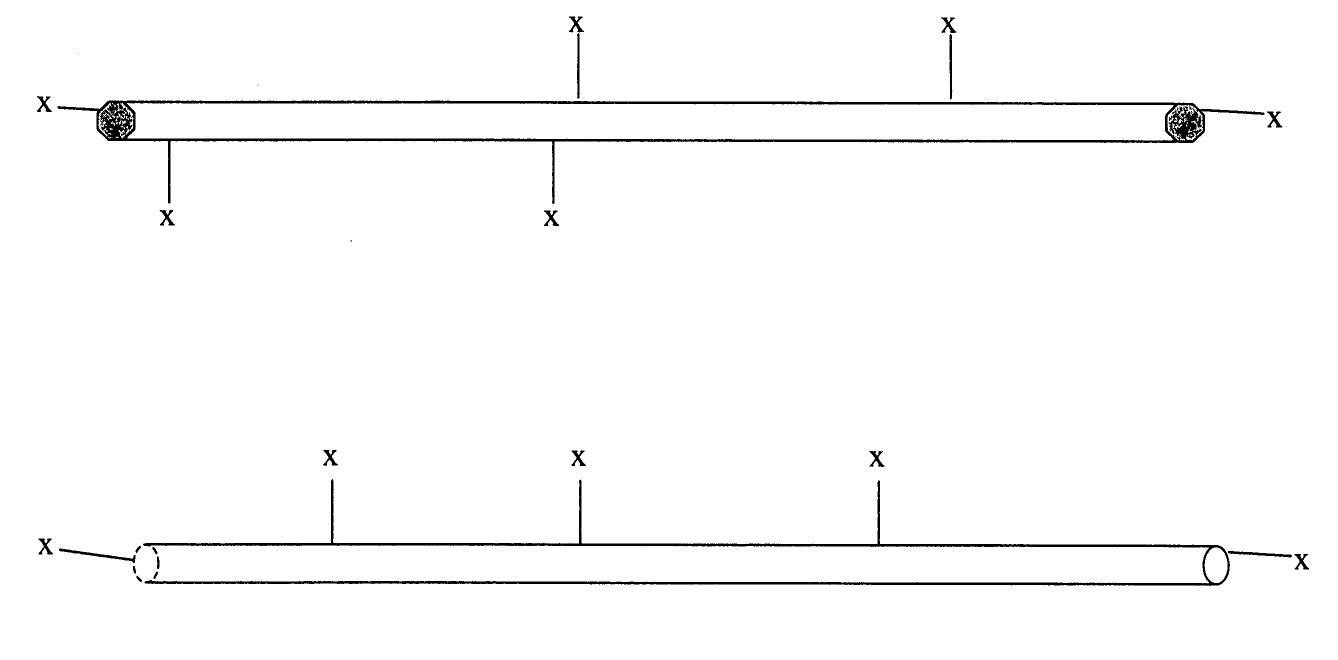
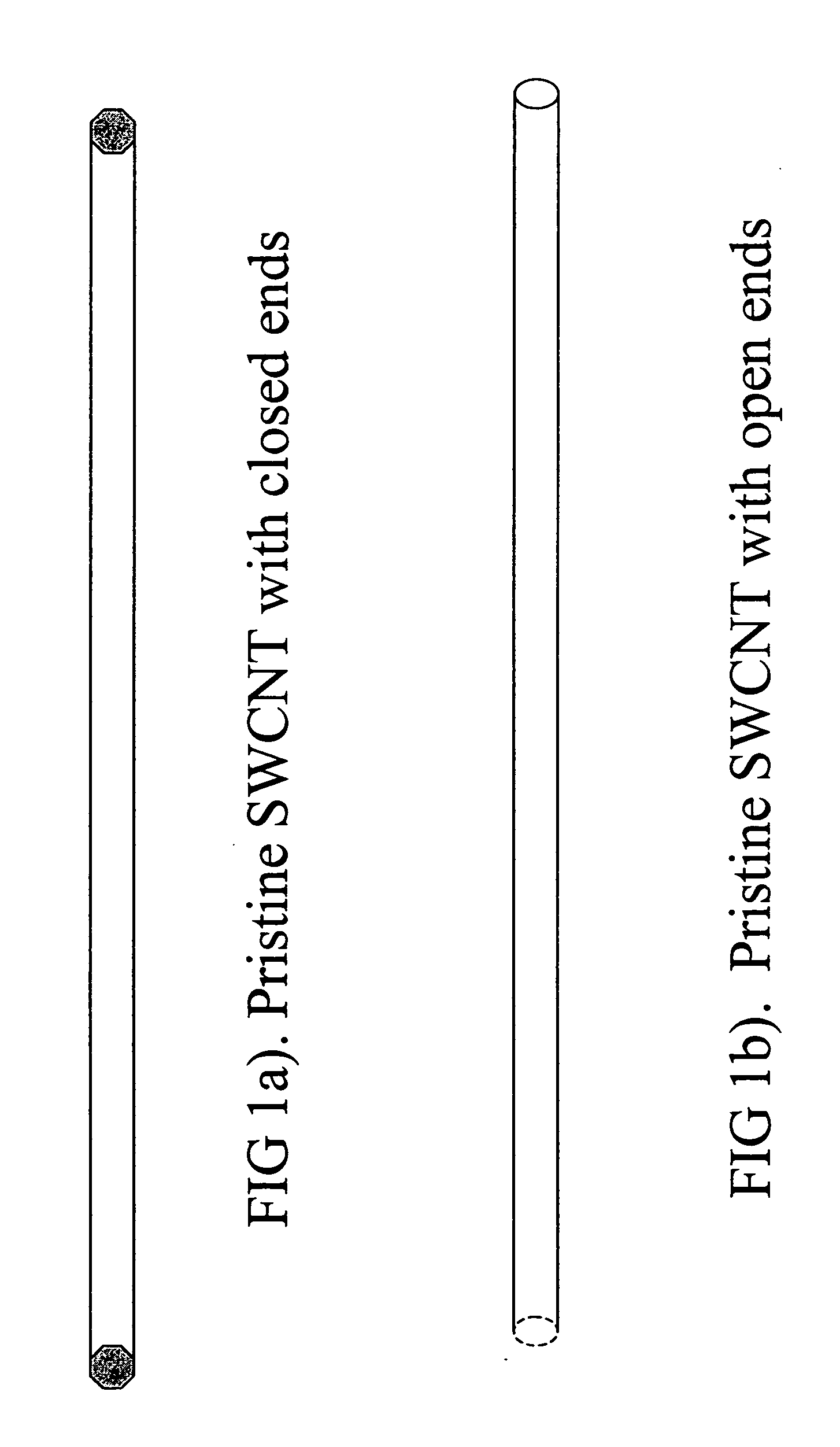
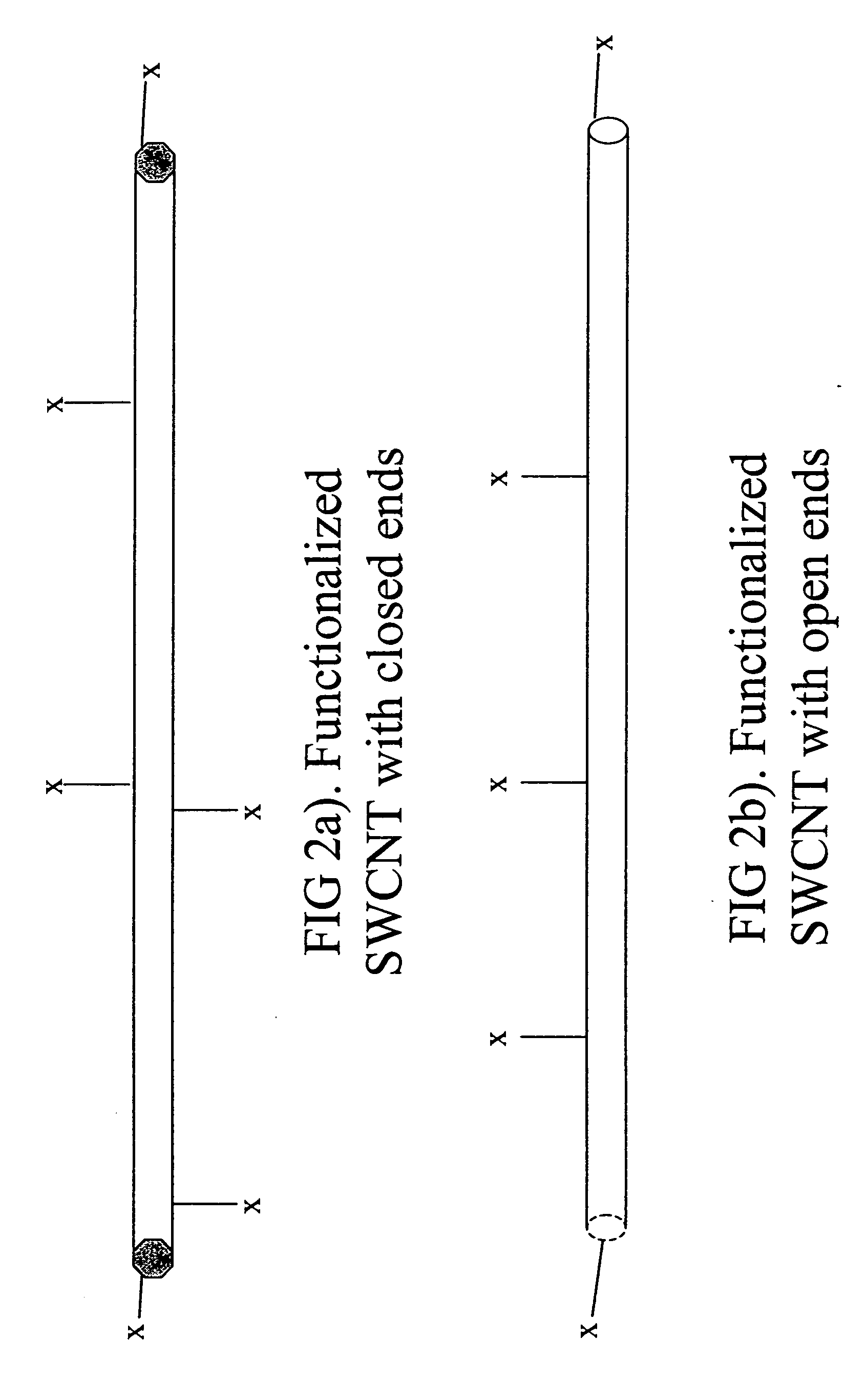
[0160] Exemplary Donor laminates with conductive layers comprising SWCNT were prepared as described herein below. The SWCNTs used in the following examples were provided by Carbon Solutions Inc. as product code P3-SWNT. These SWCNTs were coated from aqueous solutions on suitable substrates. The laminate substrate used was either photographic grade triacetylcellulose (TAC) with a thickness of 127 μm, and surface roughness Ra of 1.0 nm or photographic grade polyethylene terephthalate (PET) with a thickness of 102 μm and surface roughness Ra of 0.5 nm. In all cases the surface of the substrate was corona discharge treated prior to coating. Aqueous coating composition was applied to the corona discharge treated surface of the substrate by a hopper at different wet lay downs, and dried at 82° C. In this manner, examples of donor laminates DL-1 through DL-3 were created as per invention, wherein conductive layers of different coverage of SWCNT were coated on the sur...


PUM

PropertyMeasurementUnit
surface roughnessaaaaaaaaaa
outer diameteraaaaaaaaaa

Abstract

The present invention relates to a donor laminate for adhesive transfer of a conductive layer comprising a substrate having thereon a conductive layer comprising carbon nanotubes, in contact with said substrate

Description

FIELD OF THE INVENTION [0001] The present invention relates to a donor laminate for transfer of a conductive layer comprising carbon nanotubes on to a receiver, wherein the receiver is a component of a device. The present invention also relates to methods pertinent to such transfers. BACKGROUND OF THE INVENTION [0002] Transparent electrically-conductive layers (TCL) of metal oxides such as indium tin oxide (ITO), antimony doped tin oxide, and cadmium stannate (cadmium tin oxide) are commonly used in the manufacture of electrooptical display devices such as liquid crystal display devices (LCDs), electroluminescent display devices, photocells, solid-state image sensors, electrochromic windows and the like. [0003] Devices such as flat panel displays, typically contain a substrate provided with an indium tin oxide (ITO) layer as a transparent electrode. The coating of ITO is carried out by vacuum sputtering methods which involve high substrate temperature conditions up to 250° C., and t...

Claims


Application Information

Patent Timeline
Patent Type & Authority Applications(United States)
IPC IPC(8): B44C1/165B44C1/17B32B5/16
CPCB44C1/17B82Y20/00B82Y30/00Y10T428/2982G02F2202/16G02F2202/36G02F2201/12
Inventor IRVIN, GLEN C. JR.MAJUMDAR, DEBASISANDERSON, CHARLES C.ROWLEY, LAWRENCE A.FREEDMAN, GARY S.
Owner EASTMAN KODAK CO
Why Eureka
Try Eureka