Thin film forming method and forming device therefor

a technology of forming method and forming device, which is applied in the direction of optical elements, radio frequency controlled devices, instruments, etc., can solve the problems of difficult control of refractive index, complicated design, and difficulty in obtaining thin films with arbitrary optical characteristics, and achieve high reproducibility

Inactive Publication Date: 2006-08-24
SHINCRON KK
View PDF16 Cites 7 Cited by
  • Summary
  • Abstract
  • Description
  • Claims
  • Application Information

AI Technical Summary

Benefits of technology

[0028] In this region, since the ratio of the change of the optical characteristic is large with respect to the change of the oxygen flow rate, and the hysteresis phenomenon occurs, it is very difficult to control the optical characteristic of the formed thin film by the adjusting of the oxygen flow rate. Therefore, by the...

Problems solved by technology

However, when the optical thin film is designed using the limited materials in this manner, the design becomes complicated, and it has been difficult to obtain the thin film having arbitrary optical characteristics.
However, there has been a problem that it is difficult to control the refractive index and obtain a process having a stabilized quality in the technique for evaporating the low and high-refractive materials simultaneously from the separate evaporation sources to obtain the intermediate refractive index by the mixture ratio, the technique for mixing the low and high-refractive materials, and evaporating the materials simultaneously from one evaporation source to obtain the intermediate refractive index by the mixture ratio, the equivalent film technique for equivalently obtaining the intermediate refractive index by the combination of the ...

Method used


Image

  • Thin film forming method and forming device therefor
  • Thin film forming method and forming device therefor
  • Thin film forming method and forming device therefor

Examples


Embodiment Construction

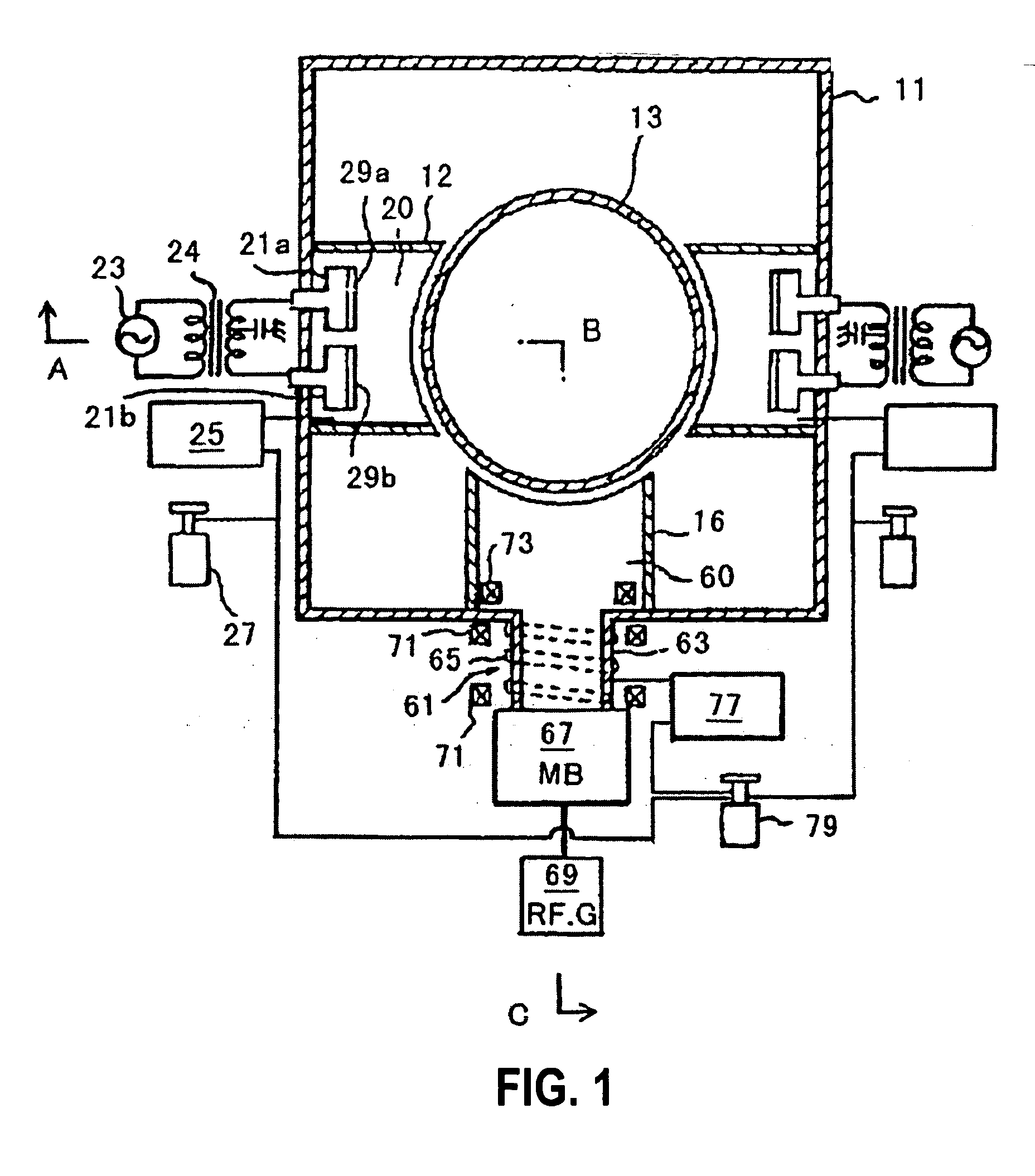
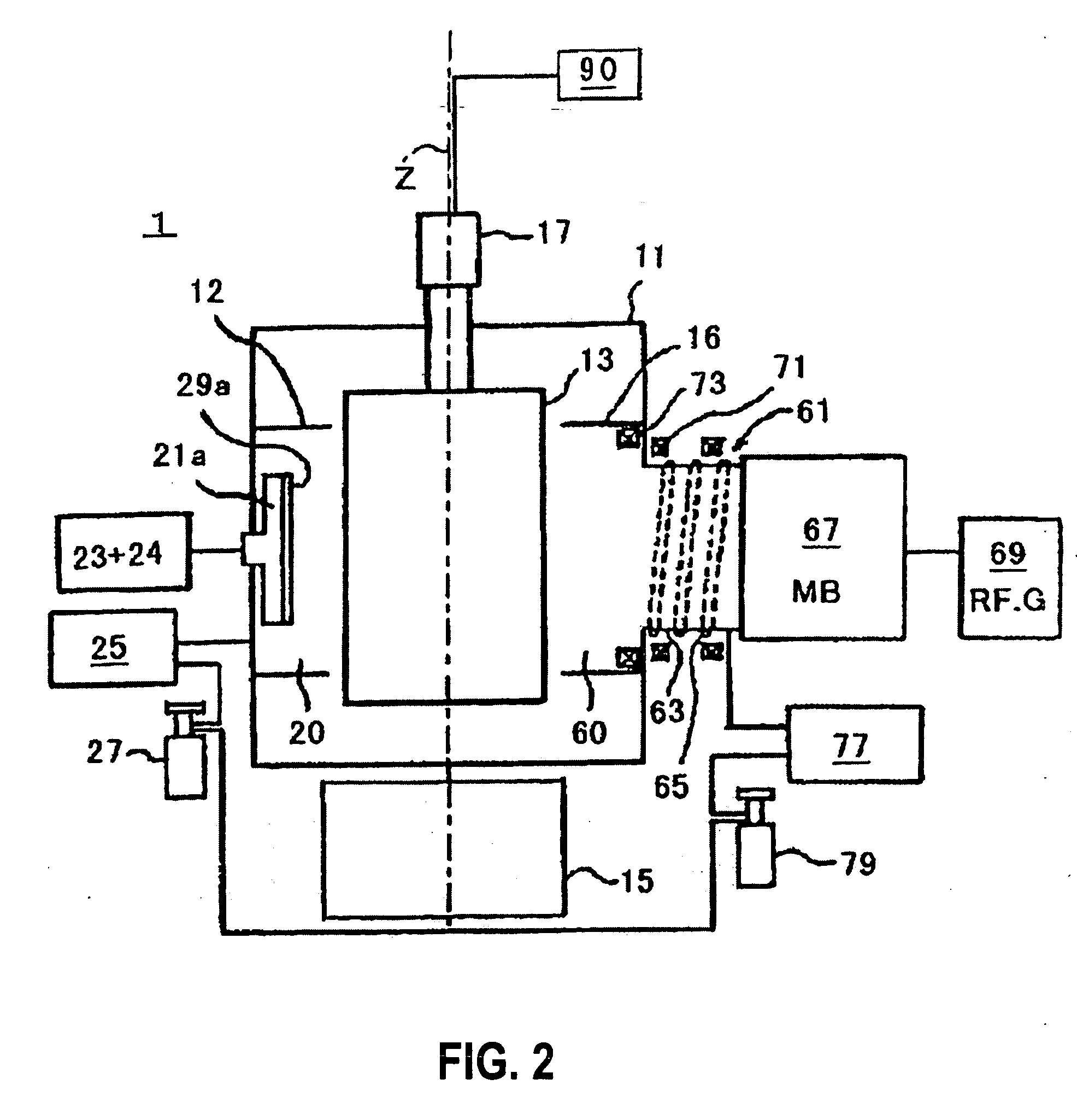
[0039] The present invention is an invention relating to a method of manufacturing a thin film and a sputtering apparatus for performing sputtering to form a thin film on a substrate. An embodiment of the present invention will be described hereinafter with reference to the drawings. It is to be noted that members, arrangement of the members and the like described hereinafter do not limit the present invention, and can be variously modified within the scope of the present invention.

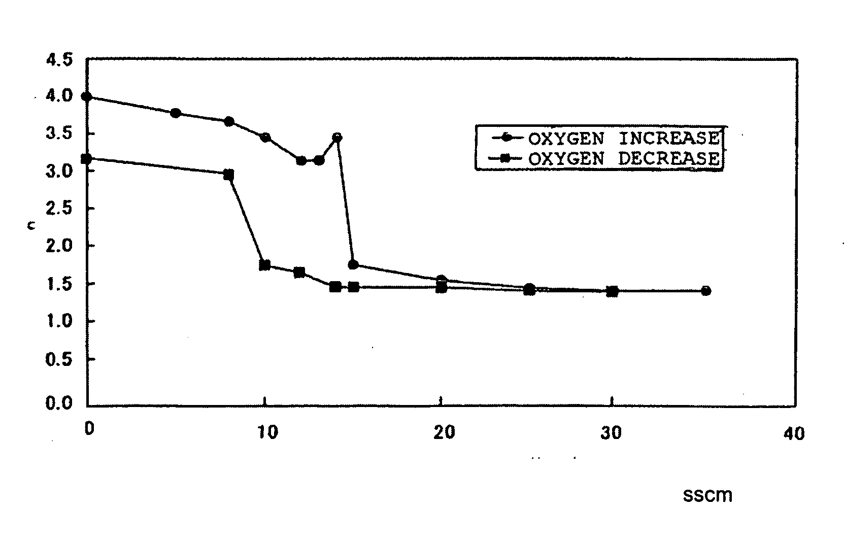
[0040] In the present embodiment, film formation and reaction of an intermediate thin film are repeatedly performed to form a thin film in order to obtain a targeted optical characteristic value and film thickness.

[0041] A range of a targeted optical characteristic value of the thin film indicate optical characteristic values in a region wherein a hysteresis phenomenon occurs in which a change route of the optical characteristic value changes with respect to a reactive gas flow rate in a case where a fl...


PUM

PropertyMeasurementUnit
Volumetric flow rateaaaaaaaaaa
Optical propertiesaaaaaaaaaa

Abstract

A method of forming a thin film of the present invention comprises: an optical characteristic adjusting step of repeatedly conveying a substrate holder between a zone to perform an intermediate thin film forming step and a zone to perform a film composition converting step while controlling a conveying speed of the substrate holder for holding a substrate, and adjusting a film composition of a finally formed thin film to form the thin film having an optical characteristic value of a region where a hysteresis phenomenon occurs.

Description

BACKGROUND OF THE INVENTION [0001] 1. Field of the Invention [0002] The present invention relates to a method of manufacturing a thin film and a sputtering apparatus, particularly to a method of manufacturing a thin film, and a sputtering apparatus in which sputtering is performed to form a thin film having desired optical characteristics on a substrate. [0003] 2. Description of the Related Art [0004] Attempts have heretofore been made to design an optical thin film using limited materials in the natural world in order to design optical spectral characteristics required for a certain product group. However, when the optical thin film is designed using the limited materials in this manner, the design becomes complicated, and it has been difficult to obtain the thin film having arbitrary optical characteristics. [0005] Therefore, it has been necessary to obtain a material having an arbitrary refractive index and decay coefficient, that is, a material which does not exist in the natura...

Claims


Application Information

Patent Timeline
IPC IPC(8): H01L21/84H01L27/148C23C16/00C23C14/34C23C14/56C23C14/58G02B1/11G02B1/115
CPCC23C14/0078C23C14/568C23C14/5846C23C14/3407
Inventor SONG, YIZHOUSAKURAI, TAKESHI
Owner SHINCRON KK
Why Eureka
Try Eureka