Fin type field effect transistors and methods of manufacturing the same

Active Publication Date: 2006-08-24
SAMSUNG ELECTRONICS CO LTD
View PDF4 Cites 57 Cited by
  • Summary
  • Abstract
  • Description
  • Claims
  • Application Information

AI Technical Summary

Benefits of technology

[0013]FIG. 1 is a cross sectional view illustrating a fin type field effect transistor in accordance with a first embodiment of the present invention;
[0014] FIGS. 2 to 14 are cross sectional views illustrating methods of manufacturing the fin type field effect transistor in FIG. 1 in accordance with some embodiments of the present invention;

Problems solved by technology

As semiconductor devices have become highly integrated, the gate length of horizontal field effect transistors has become shorter and led to problems associated with short channel effects.
However, when an upper silicon layer of the SOI substrate has a non-uniform thickness, the threshold voltage of the transistor can be readily changed.
Further, the driving current can be deteriorated due to a self-heating

Method used


Image

  • Fin type field effect transistors and methods of manufacturing the same
  • Fin type field effect transistors and methods of manufacturing the same
  • Fin type field effect transistors and methods of manufacturing the same

Examples


embodiment 1

[0024]FIG. 1 is a cross sectional view illustrating a fin type field effect transistor in accordance with a first embodiment of the present invention.

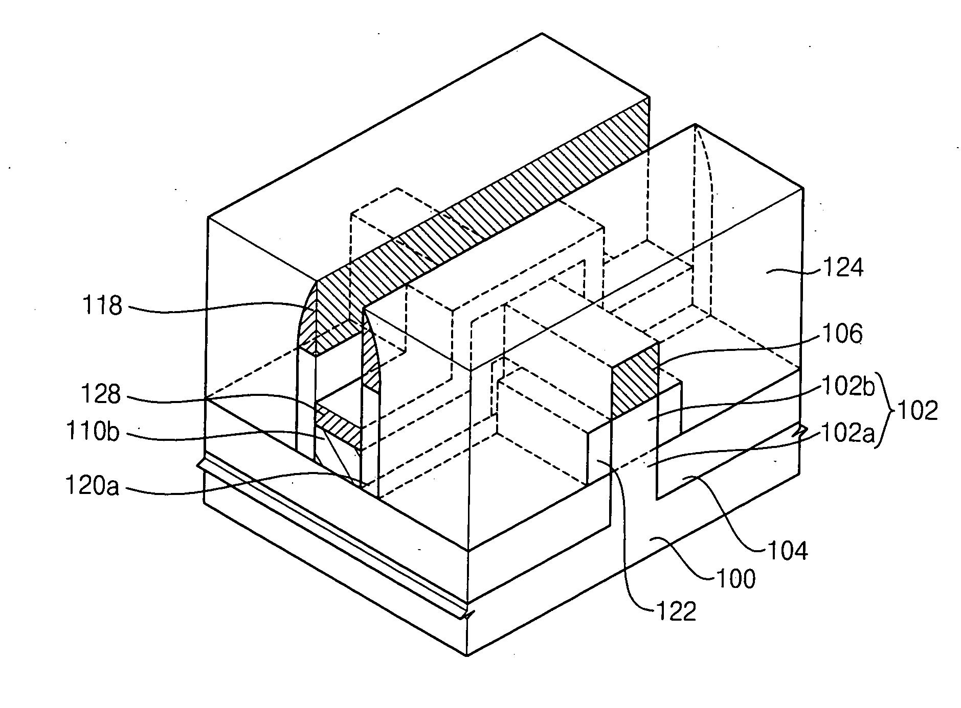
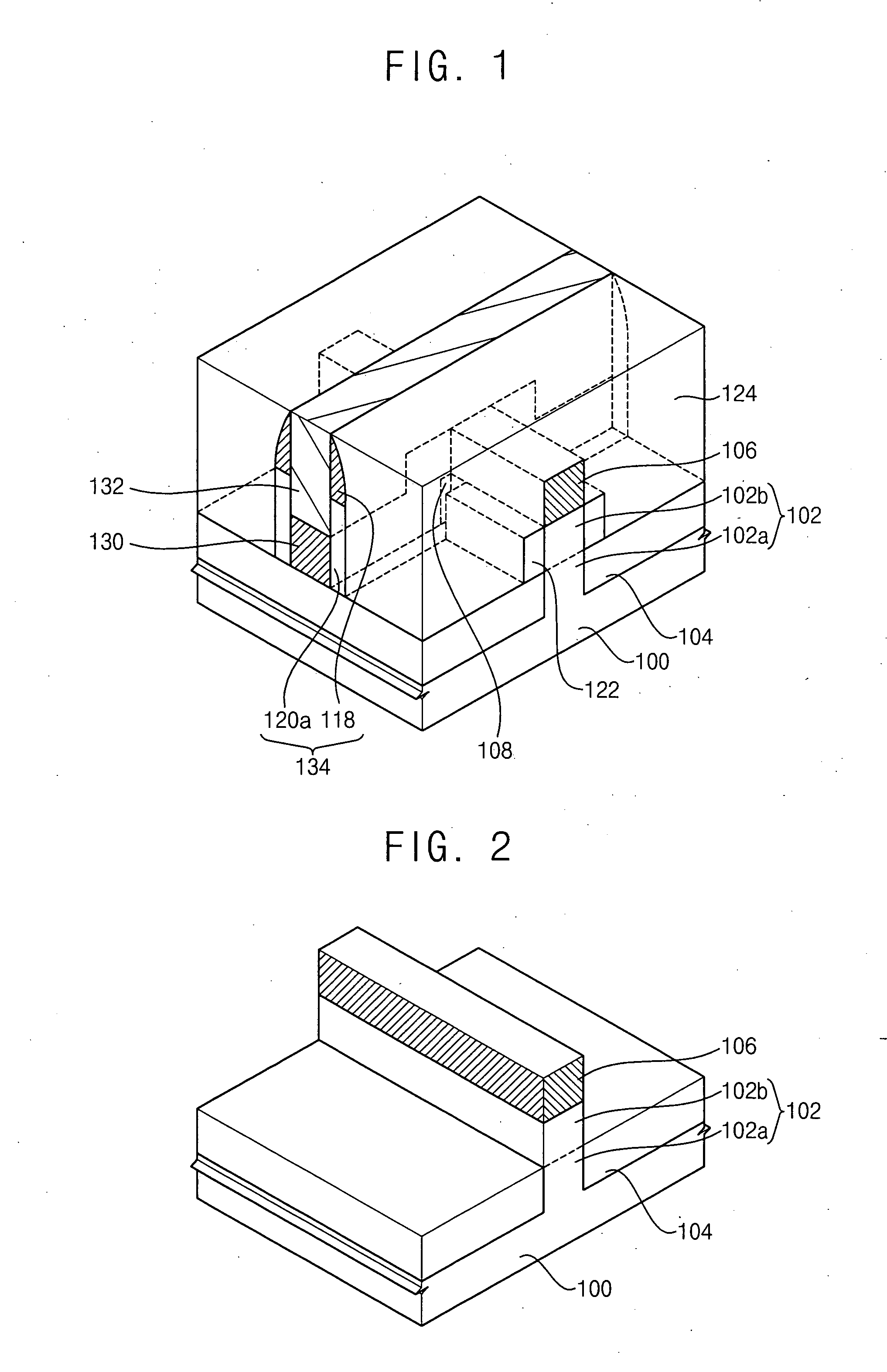
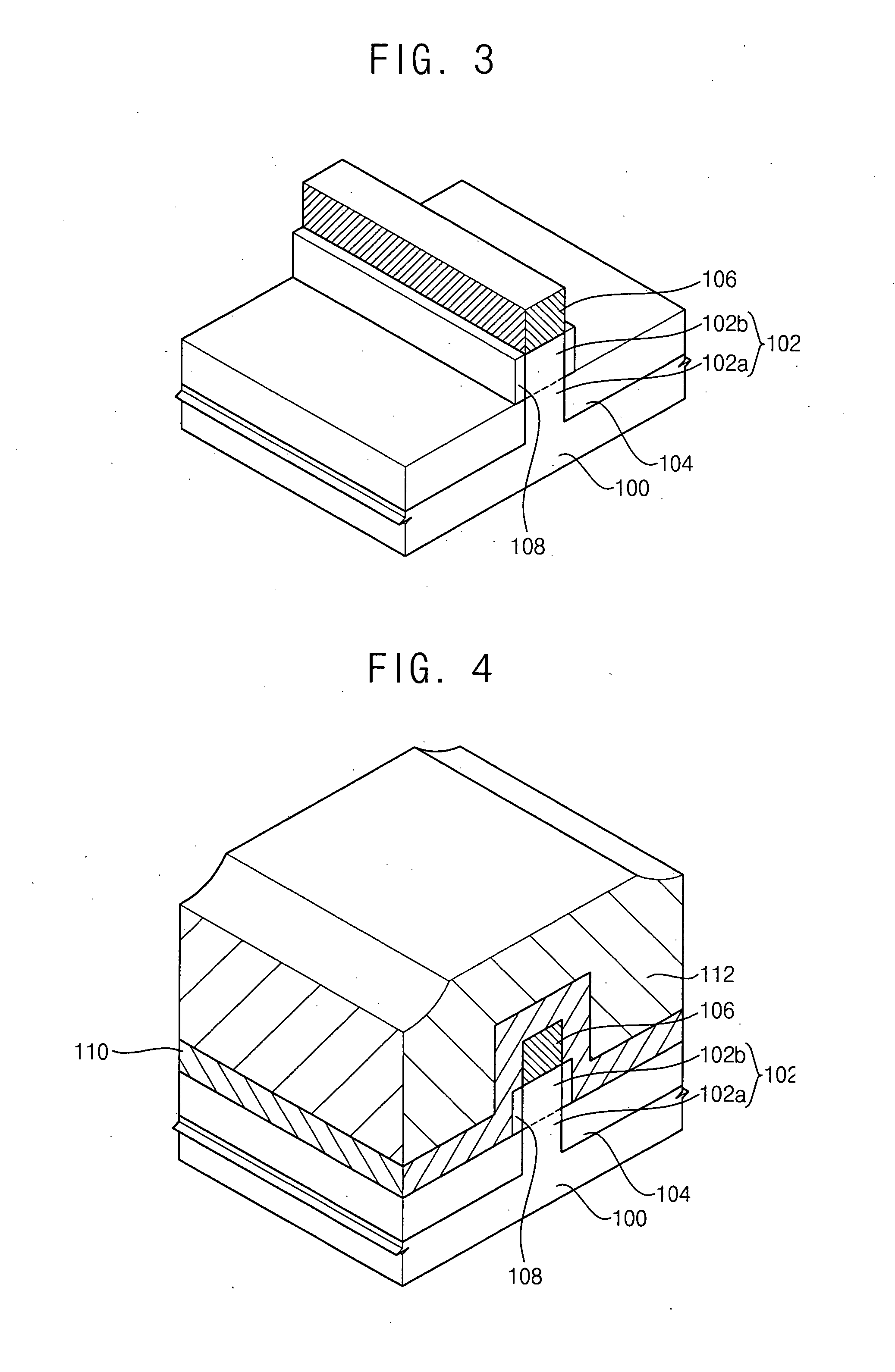
[0025] Referring to FIG. 1, an active fin 102 is formed on a surface of a semiconductor substrate 100 including silicon. The active fin 102 extends away from a major surface of the semiconductor substrate 100. The active fin 102 can be integrally formed with the semiconductor substrate 100, so that the active fin 102 can be formed from the same, or substantially the same, material as the semiconductor substrate 100. In some embodiments, the active fin 102 may have a width of no more than about 40 nm to allow control of a gate electrode formed on opposite sides of the active fin 102.

[0026] An isolation layer 104 is formed on the semiconductor substrate 100 to electrically isolate unit devices, which are formed on the active fin 102, from each other. The thickness of the isolation layer 104 is defined so that an upper portion of the ac...

embodiment 2

[0091]FIG. 15 is a cross sectional view illustrating a fin type field effect transistor in accordance with a second embodiment of the present invention.

[0092] The exemplary fin type field effect transistor includes elements substantially identical to those in Embodiment 1 except for an SOI substrate. Accordingly, the same reference numerals are used to refer to the same elements and any further illustration and explanation with respect to the same elements is omitted herein for brevity.

[0093] Referring to FIG. 15, an active fin 202 is formed on the SOI substrate 200 including a silicon layer 200a and a buried oxide layer 200b sequentially stacked. Thus, the active fin 202 is not electrically connected to the silicon layer 200a of the SOI substrate 200. The fin type field effect transistor is formed on the active fin 202 and the buried oxide layer 200b using, for example, the methods described below.

[0094]FIG. 16 is a cross sectional view illustrating methods of manufacturing the ...


PUM


Abstract

A fin type field effect transistor includes a semiconductor substrate, an active fin, a first hard mask layer pattern, a gate insulation layer pattern, a first conductive layer pattern, and source/drain regions. The active fin includes a semiconductor material and is formed on the substrate and extends in a direction away from a major surface of the substrate. The first hard mask layer pattern is formed on a distal surface of the active fin from the substrate. The gate insulation layer is formed on a sidewall portion of the active fin. The first conductive layer pattern includes a metal silicide and is formed on surfaces of the substrate and the gate insulation layer pattern, and on a sidewall of the first hard mask pattern. The source/drain regions are formed in the active fin on opposite sides of the first conductive layer pattern.

Description

CROSS REFERENCE TO RELATED APPLICATION [0001] This application claims priority under 35 USC § 119 to Korean Patent Application No. 10-2005-0015221, filed on Feb. 24, 2005, the contents of which are herein incorporated by reference in their entirety. FIELD OF THE INVENTION [0002] The present invention relates to field effect transistors and methods of manufacturing field effect transistors and, more particularly, to a field effect transistor formed on an active fin and methods of manufacturing the same. BACKGROUND OF THE INVENTION [0003] As semiconductor devices have become highly integrated, the gate length of horizontal field effect transistors has become shorter and led to problems associated with short channel effects. Short channel effects can be associated with reduced electromigration and driving current due to increased impurity concentration in a channel layer of the horizontal field effect transistor. Junction leakage current can also be increased due to shallow junction de...

Claims


Application Information

Patent Timeline
IPC IPC(8): H01L21/8234H01L29/76
CPCH01L29/66545H01L29/66795H01L29/785H01L29/78618H01L21/18H01L21/24
Inventor LEE, JONG-WOOKLEE, DEOK-HYUNGKANG, MIN-GUSHIN, YU-GYUN
Owner SAMSUNG ELECTRONICS CO LTD
Why Eureka
Try Eureka