Ta-TaN selective removal process for integrated device fabrication

Active Publication Date: 2006-08-24
TAIWAN SEMICON MFG CO LTD
View PDF8 Cites 29 Cited by
  • Summary
  • Abstract
  • Description
  • Claims
  • Application Information

AI Technical Summary

Benefits of technology

[0011] In this first use, XeF2 is used to remove the metal liner, TaN—Ta, after copper CMP to minimize mechanical stressing of the low k material and chemical alteration of the low k dielectric material, and to improve planarity after CMP. In the second use, the XeF2 etch is used to selectively remove a plating base (TaN—Ta) that was used to form a metal cap layer over the copper conductor. In this use, the metal cap allows the elimination of a high k dielectric cap normally required to prevent diffusion of copper into the interconnect dielectric.

Problems solved by technology

These materials have been extremely challenging to implement because they are mechanically weak and chemically sensitive to many of the processes used to integrate BEOL structures.
Mechanical damage, water penetration and slurry incorporation can all cause permanent damage to the low k dielectric.
Furthermore, some dielectric materials are used in BEOL devices as integration or reliability enhancement layers and are detrimental to maintaining a low k BEOL structure.

Method used


Image

  • Ta-TaN selective removal process for integrated device fabrication
  • Ta-TaN selective removal process for integrated device fabrication
  • Ta-TaN selective removal process for integrated device fabrication

Examples


second embodiment

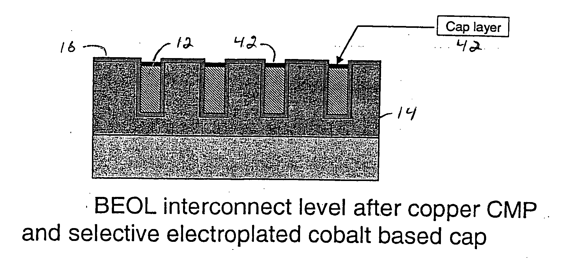
[0024] In a second embodiment, illustrated in FIGS. 4A and 4B, the XeF2 etch is used to remove a plating base required for selective metal cap 42 formation over the copper conductor 12. This process has been tested to show that only the plating base is etched and the metal cap 42 and surrounding dielectric 14 are preserved. Long XeF2 etch tests with cobalt based cap layers showed only a 7% sheet resistance increase which could be due to some impurity incorporation on the surface or a 7% thickness loss.

[0025] Furthermore, we have also tested the compatibility of XeF2 with copper and found that no etching occurs.

third embodiment

[0026] In a third embodiment, the XeF2 etch is used to remove the plating base / liner for a non-planar structure fabricated by through mask plating or by the combination of damascene and through mask plating. A high performance thick copper inductor is a typical example of a device that could be fabricated in this manner.

[0027]FIGS. 5A-5H depict the combined process flow that results in a non-planar structure, which renders plating base / liner removal by CMP impossible. In accordance with the third embodiment of the invention, the selective removal of the TaN / Ta plating base / liner can be done either directly after resist strip or following selective passivation of the exposed copper.

[0028]FIG. 5A shows a starting structure BEOL interconnect on a semiconductor device. More specifically, FIG. 5A shows a substrate 52 with semiconductor devices, dielectric material 54 on that substrate, and copper regions 56 embedded in the dielectric. TaN—Ta liners 60 separate these copper regions from ...


PUM


Abstract

Disclosed are a method and a system for processing a semiconductor structure of the type including a substrate, a dielectric layer, and a TaN—Ta liner on the dielectric layer. The method comprises the step of using XeF2 to remove at least a portion of the TaN—Ta liner completely to the dielectric layer. In the preferred embodiments, the present invention uses XeF2 selective gas phase etching as alternatives to Ta—TaN Chemical Mechanical Polishing (CMP) as a basic “liner removal process” and as a “selective cap plating base removal process.” In this first use, XeF2 is used to remove the metal liner, TaN—Ta, after copper CMP. In the second use, the XeF2 etch is used to selectively remove a plating base (TaN—Ta) that was used to form a metal cap layer over the copper conductor.

Description

BACKGROUND OF THE INVENTION [0001] 1. Field of the Invention [0002] This invention generally relates to integrated device fabrication; and more specifically, the invention relates to selective removal processes for integrated device fabrication. Even more specifically, the invention relates to processes that may be used effectively to remove selectively Ta—TaN layers or liners during the fabrication of an integrated device and that are compatible with low k dielectric materials. [0003] 2. Background Art [0004] Generally, in the fabrication of integrated devices, various layers of materials, including copper and dielectric materials, are formed and patterned or etched to produce the desired end product. For example, Back-End-Of-Line (BEOL) interconnects are commonly fabricated using a combination of sequential layering and patterning of metal and dielectric films to produce an integrated multilevel wiring architecture for various semiconductor devices. [0005] Advanced semiconductor d...

Claims


Application Information

Patent Timeline
IPC IPC(8): H01L21/44H01L23/48
CPCH01L21/32135H01L21/306H01L21/76843H01L21/76849H01L21/76865H01L23/5227H01L23/53238H01L24/11H01L2224/13099H01L2924/01002H01L2924/01018H01L2924/01022H01L2924/01027H01L2924/01029H01L2924/01042H01L2924/01054H01L2924/01073H01L2924/01074H01L2924/01078H01L2924/04953H01L2924/19042H01L2924/30105H01L2924/01006H01L2924/01019H01L2924/01033H01L21/7684H01L2924/14H01L2924/00
Inventor COTTE, JOHN MICHAELHOIVIK, NILS DENEKEJAHNES, CHRISTOPHER VINCENTWISNIEFF, ROBERT LUKE
Owner TAIWAN SEMICON MFG CO LTD
Why Eureka
Try Eureka