Multi-band low noise amplifier, multi-band low noise amplifier module, wireless integrated circuit and multi-band RF module

a low noise amplifier and amplifier module technology, applied in the field of multi-band wireless communication, can solve the problems of shortening the available frequency in the existing rf band, and achieve the effect of reducing the size of the wireless semiconductor integrated circui

Inactive Publication Date: 2006-08-24
RENESAS TECH CORP
View PDF4 Cites 96 Cited by
  • Summary
  • Abstract
  • Description
  • Claims
  • Application Information

AI Technical Summary

Benefits of technology

[0040] According to the invention, since a plurality of RF bands can share a low...

Problems solved by technology

Also, if the communication speeds of mobile phones increase, a shortage of available frequenc...

Method used


Image

  • Multi-band low noise amplifier, multi-band low noise amplifier module, wireless integrated circuit and multi-band RF module
  • Multi-band low noise amplifier, multi-band low noise amplifier module, wireless integrated circuit and multi-band RF module
  • Multi-band low noise amplifier, multi-band low noise amplifier module, wireless integrated circuit and multi-band RF module

Examples


first embodiment

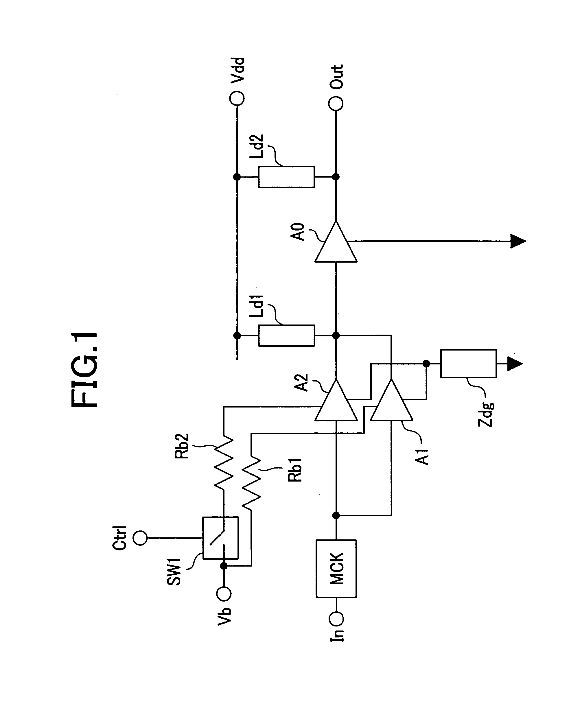
[0058]FIG. 1 shows a multi-band low noise amplifier LNA adaptable to two RF bands including a high-band HB and a low-band LB, as a first embodiment of the invention.

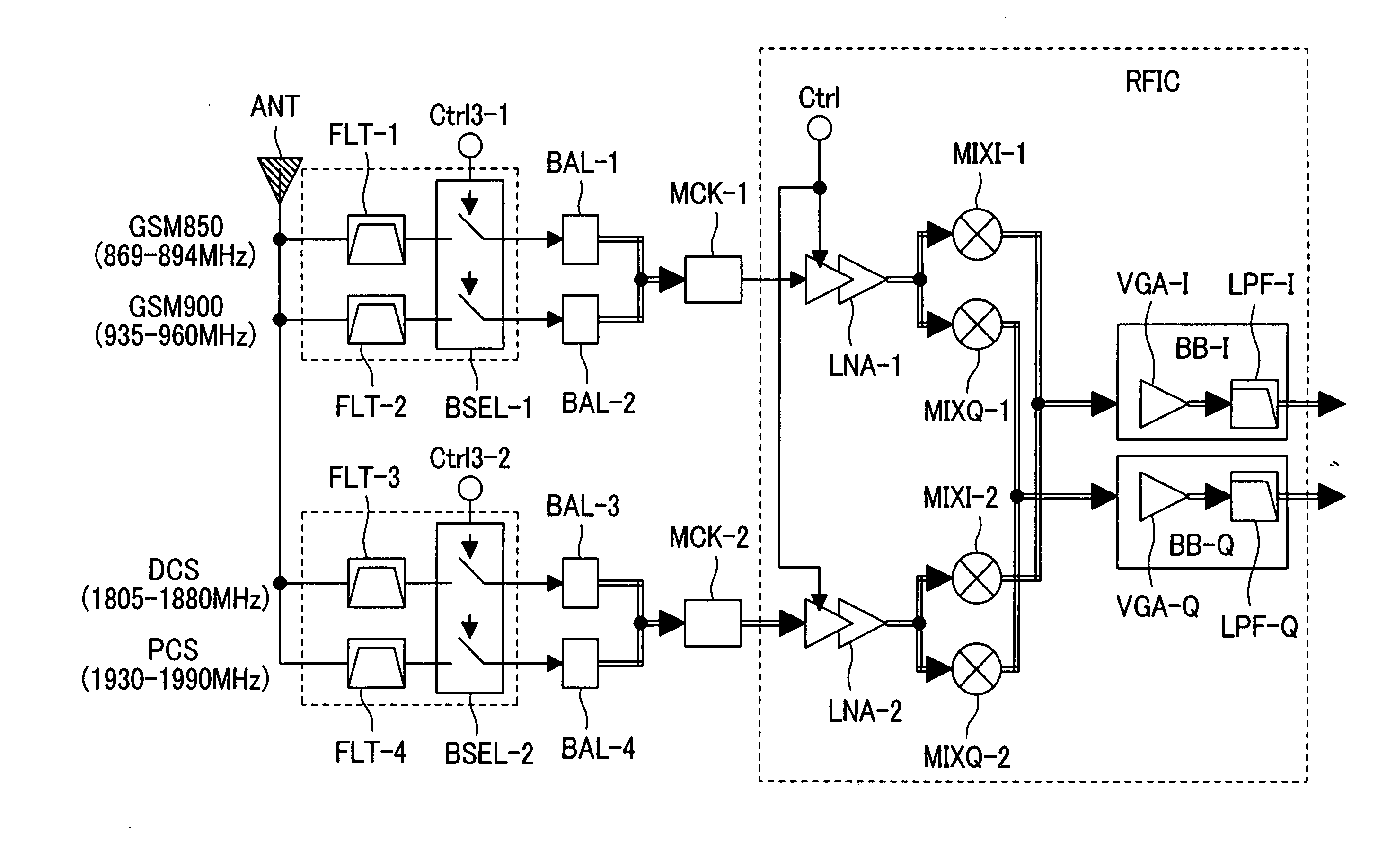
[0059] Only the main part of the LNA is shown here to simplify illustration. Illustration of the antenna ANT, the antenna switch and the band pass filters FLT arranged on the input side of the LNA and the mixers MixI and MixQ, the local frequency synthesizer, the baseband circuit, and the control circuit for frequency band selection arranged on the input side of the LNA is dispensed with.

[0060] The LNA of this embodiment has a pre-stage amplification unit comprising first and second fundamental amplifiers A1 and A2 connected in parallel to each other. These fundamental amplifiers share a load impedance Ld1 connected to a source voltage Vdd, a grounded degeneration impedance Zdg and an input impedance matching circuit MCK. A bias voltage Vb for turning on the fundamental amplifiers A1 and A2 is supplied to the first fun...

second embodiment

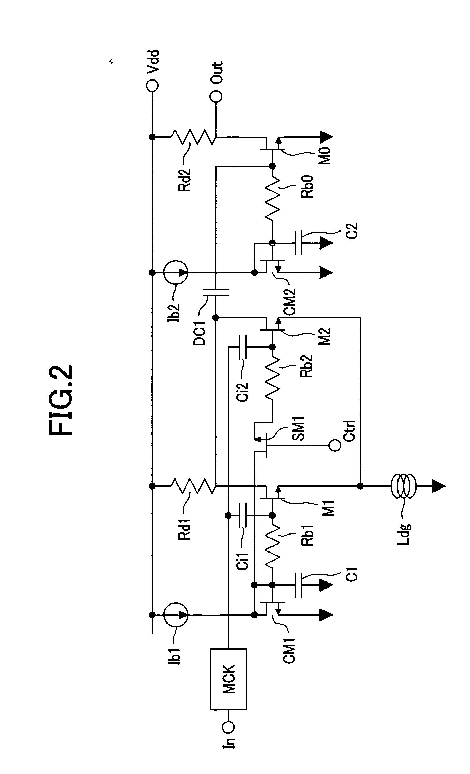
[0063]FIG. 2 shows the main part of a multi-band low noise amplifier LNA adaptable to two RF bands including a high-band HB and a low-band LB, as a second embodiment of the invention. As in the first embodiment, the circuit elements connected to the input and output sides of the multi-band LNA are not shown here for the sake of simplification of illustration.

[0064] The multi-band LNA of this embodiment has a pre-stage amplification unit comprising first and second field effect transistors M1 and M2 connected in parallel, and these field effect transistors share a load resistor Rd1 connected to the source voltage Vdd, a grounded degeneration inductance Ldg and the input impedance matching circuit MCK. Capacitor elements Ci1 and Ci2 for separating DC potentials are inserted between MCK and the first and second field effect transistors M1 and M2.

[0065] A bias voltage Vb for turning on the first and second field effect transistors M1 and M2 is supplied from a first current mirror circ...

third embodiment

[0080]FIG. 5 shows the main part of a multi-band LNA adaptable to three RF bands including a high band (HB), a mid-band (MB) and a low-band (LB) as a third embodiment of the invention. As was the case with the first embodiment, the circuit elements connected to the input and output sides of the multi-band LNA are not shown here for the sake of simplification of illustration.

[0081] In the multi-band LNA of this embodiment, a third fundamental amplifier A3 is further connected in parallel to the first and second fundamental amplifiers A1 and A2 constituting the pre-stage amplification unit of the first embodiment (FIG. 1). These three fundamental amplifiers share the load impedance Ld1 connected to the source voltage Vdd, the grounded degeneration impedance Zdg and the input impedance matching circuit MCK.

[0082] The bias voltage Vb for turning on the fundamental amplifiers is supplied all the time to the first fundamental amplifier A1 through the first bias resistor Rb1, selectively...


PUM


Abstract

A multi-band radio module for selectively supplying received signals in a plurality of frequency bands to a low noise amplifier via an input impedance matching circuit by switching over the operation mode of the low noise amplifier is comprised of: a pre-stage amplification unit including a plurality of fundamental amplifiers connected to one another in parallel, the fundamental amplifiers sharing a load impedance connected to a source voltage and a grounded degeneration impedance and having input signal lines commonly connected to an input impedance matching circuit; a post-stage amplifier to which the output signals of the plurality of fundamental amplifiers are commonly inputted; and a bias control unit for selectively turning on the fundamental amplifiers, wherein the input impedance of the low noise amplifier is selectively optimized for the matching circuit depending on the RF band to be received.

Description

CLAIM OF PRIORITY [0001] The present application claims priority from Japanese application serial No. 2005-045637, filed on Feb. 22, 2005, the content of which is hereby incorporated by reference into this application. FIELD OF THE INVENTION [0002] The present invention relates to a multi-band wireless communication technology which selectively uses a plurality of radio frequency (RF) bands, and more particularly to a multi-band low noise amplifier adaptable to a plurality of RF bands, and a wireless semiconductor integrated circuit (RF-IC), a multi-band low noise amplifier module and a multi-band RF module to which the amplifier is applied. BACKGROUND OF THE INVENTION [0003] In prior art of RF-ICs for mobile phones, an RF-IC having also the function of communicating with wireless LANs and an RF-IC having also the function for Blootooth that uses the same 2.4 GHz band as IEEE 802.11b / g wireless LAN are known, for instance, as proposed in: Manku, et al., “A single chip direct convers...

Claims


Application Information

Patent Timeline
IPC IPC(8): H04B7/00H04B7/08H03D5/00H04B1/06
CPCH03F3/19H03F3/1935H03F3/72H03F2200/111H03F2200/294H03F2200/372H04B1/0053H04B1/0458
Inventor KYU, IREITANAKA, SATOSHIMAEDA, KOJIAKAMINE, YUKINORI
Owner RENESAS TECH CORP
Why Eureka
Try Eureka