Multilayer mirror, method for manufacturing the same, and exposure equipment

a multi-layer mirror and manufacturing method technology, applied in the field of multi-layer mirrors, can solve the problem of restricted number of apertures (na) in the optical system, and achieve the effect of reducing the incidence angle dependence of reflectivity

Active Publication Date: 2006-08-31
NIKON CORP
View PDF9 Cites 30 Cited by
  • Summary
  • Abstract
  • Description
  • Claims
  • Application Information

AI Technical Summary

Benefits of technology

[0046] An object of the present invention is to provide a technique for reducing the incidence angle dependence of the reflectivity on a multilayer mirror etc.

Problems solved by technology

In a projection optical system using a lens, it is possible to realize an optical system in which light advances in one direction along the optical axis, however, in a projection optical system configured by a mirror, a flux of light is turned back many times. Due to this, it becomes necessary to prevent the turned back flux of light from interfering with a mirror substrate spatially and the numerical aperture (NA) in the optical system is restricted.

Method used


Image

  • Multilayer mirror, method for manufacturing the same, and exposure equipment
  • Multilayer mirror, method for manufacturing the same, and exposure equipment
  • Multilayer mirror, method for manufacturing the same, and exposure equipment

Examples


embodiment 1

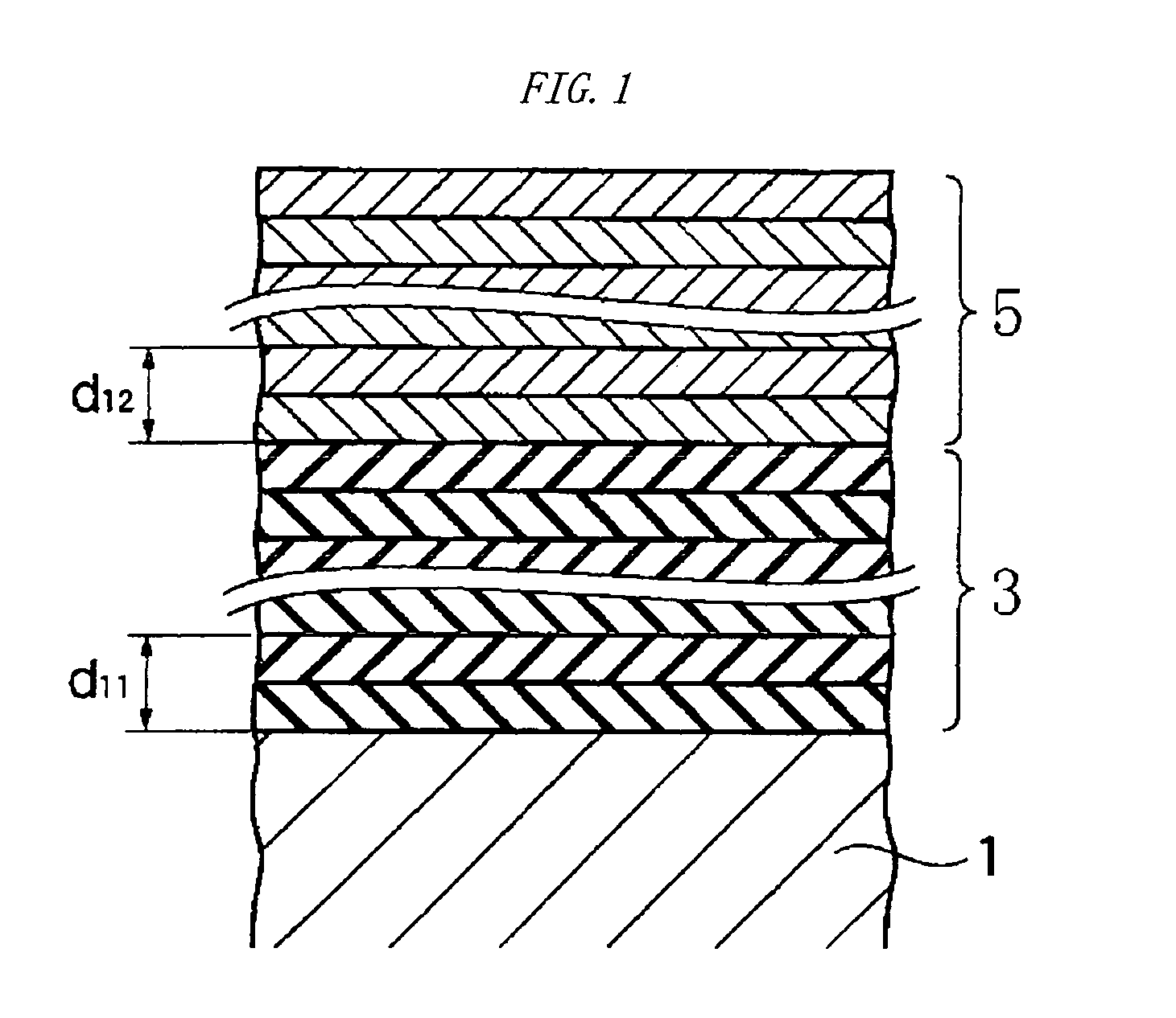
[0107]FIG. 1 is a sectional schematic diagram of a multilayer mirror according to a first embodiment of the present invention. A substrate 1 is made of low thermal expansion glass polished until the roughness of the surface (the upper surface in the drawing) is 0.2 nm RMS or less. On the surface of the substrate 1, 20 pair layers of Ru / Si multilayer 3 are formed and on the Ru / Si multilayer 3, five pair layers of Mo / Si multilayer 5 are formed. The periodic length (the thickness of unit periodic structure (layer pair) of Ru / Si, denoted by d11 in the drawing) of the Ru / Si multilayer 3 is 6.86 nm and the periodic length (the thickness of the layer pair of Mo / Si, denoted by d12 in the drawing) of the Mo / Si multilayer 5 is 6.9 nm. The value of these multilayers is 0.4 in each unit periodic structure. Note that, the value is a ratio (=dRu / d, or =dMo / d) of the thickness (dRu, or dMo) of the Ru layer or Mo layer to the periodic length (d) of the multilayer.

[0108] Here, a method for manufa...

embodiment 2

[0113]FIG. 4 is a sectional schematic diagram of a multilayer mirror according to a second embodiment of the present invention. A substrate 10 is made of low thermal expansion glass polished until the roughness of the surface (the upper surface in the drawing) is 0.2 nm RMS or less. On the surface of the substrate 10, four pair layers of Mo / Si multilayer (deep layer film group) 11 are formed. The periodic length of the Mo / Si multilayer 11 (the thickness of the pair layer of Mo / Si) is 6.9 nm and the value is 0.5.

[0114] On the surface of the Mo / Si multilayer 11, an additional layer 12 (in the present embodiment, a silicon layer) is formed. The thickness of the additional layer 12 is adjusted so as to have an optical thickness of about one-fourth of the wavelength of incidence light. In the present embodiment, the thickness of the additional layer 12 is about 3.5 nm. Further, on the surface of the additional layer 12, 20 pair layers of Mo / Si multilayer (surface layer film group) 13 h...

embodiment 3

[0120]FIG. 6 is a sectional schematic diagram of a multilayer mirror according to a third embodiment of the present invention. A substrate 20 is made of low thermal expansion glass polished until the roughness of the surface (the upper surface in the drawing) is 0.2 nm RMS or less. On the surface of the substrate 20, five pair layers of Ru / Si multilayer (deep layer film group) 21 are formed. The periodic length of the Ru / Si multilayer 21 (the thickness of the pair layer of Ru / Si) is 6.9 nm and the value is 0.5.

[0121] On the surface of the Ru / Si multilayer 21, an additional layer 22 (in the present embodiment, a silicon layer) is formed. The thickness of the additional layer 22 is adjusted so as to have an optical thickness of about one-fourth of the wavelength of incidence light. In the present embodiment, the thickness of the additional layer 22 is about 3.85 nm.

[0122] Further, on the surface of the additional layer 22, 20 pair layers of Ru / Si multilayer (surface layer film grou...


PUM

PropertyMeasurementUnit
reflectivityaaaaaaaaaa
incidence angleaaaaaaaaaa

Abstract

A multilayer mirror aims to reduce incidence angle dependence of reflectivity. A substrate is made of low thermal polished expansion glass with 0.2 nm RMS or less roughness of the surface. On the surface thereof formed is a Ru / Si multilayer having a wide full-width half maximum of peak reflectivity, and on the Ru / Si multilayer formed is a Mo / Si multilayer having a high peak reflectivity value. This enables higher reflectivity than when Ru / Si alone provided and a reflectivity peak having a wider full-width half maximum than when the Mo / Si multilayer alone provided. Since Ru absorbs EUV ray more than Mo does, higher reflectivity is obtainable than that of a structure having the Ru / Si multilayer formed on the Mo / Si multilayer. The multilayer with a wide full-width half maximum has small incidence angle dependence of reflectivity in spectral reflectivity, thereby achieving high imaging performance in projection optical system.

Description

CROSS REFERENCE TO RELATED APPLICATION [0001] This application is a continuation application of International Application PCT / JP 2004 / 015284, filed Oct. 15, 2004, designating the U.S., and claims the benefit of priority from Japanese Patent Application Nos. 2003-354561, 2003-354568, and 2003-354989, all filed on Oct. 15, 2003, and No. 2004-094633, filed on Mar. 29, 2004, the entire contents of which are incorporated herein by reference.BACKGROUND OF THE PRIOR ART [0002] 1. Technical Field [0003] The present invention relates to a multilayer mirror etc. used in EUV lithography and, more particularly, to a technique for reducing the incidence angle dependence of the reflectivity on the surface of a mirror. [0004] 2. Background of the Prior Art [0005] At present, as a method for manufacturing a semiconductor integrated circuit, reduced projection exposure capable of obtaining a high processing speed is widely utilized. In the reduced projection technique, as the semiconductor integrate...

Claims


Application Information

Patent Timeline
Patent Type & Authority Applications(United States)
IPC IPC(8): G21G5/00A61N5/00G02B5/08G02B5/26G02B5/28G03F7/20G21K1/06H01L21/027
CPCB82Y10/00G02B5/0891G03F7/70316G03F7/70958G21K1/062G03F7/70058
Inventor KANDAKA, NORIAKIMURAKAMI, KATSUHIKOKOMIYA, TAKAHARUSHIRAISHI, MASAYUKI
Owner NIKON CORP
Why Eureka
Try Eureka