Method for manufacturing electrical contact element for testing electro device and electrical contact element thereby

Inactive Publication Date: 2006-08-31
PHICOM CORP
View PDF11 Cites 16 Cited by
  • Summary
  • Abstract
  • Description
  • Claims
  • Application Information

AI Technical Summary

Benefits of technology

[0030] Accordingly, the present invention has been made in an effort to solve the problems occurring in the related art, and an object of the present invention is to provide a method for manufacturing an electrical contact element used to test an electronic device, which can overcome the problem of the conventional

Problems solved by technology

However, the conventional electrical contact element has a problem in that, since the tip portion has the pointed distal end, while the tip portion of the electrical contact element is repeatedly brought into contact with the pad of the semiconductor chip by constant physical force F, the tip portion is likely to pierce an oxide film formed on the pad and damage the pad, by which a defective proportion cannot but be increased when implementing subsequent semiconductor manufacturing processes such as a wire bonding process, and the like.
Further, due to the fact that the tip portion of the conventional electrical contact element is cornered several times at its side, while the tip portion is brought into contact with the pad of the semiconductor chip, the tip portion is apt to become worn and produce particles by itself, which contaminate the highly integrated semiconductor chip.
Also, because the tip portion of the electrical contact element has the pointed distal end, a contact area between the tip portion and the semiconductor chip pad cannot but be decreased, and thereby electric conductivity is reduced.
Moreover, while the electrical contact element must be brought into contact with the semiconductor chip pad by constant physical force F to secure the desired OD characteristic, since the tip portion has a short length, it is difficult to properly adjust the OD characteristic.
That is to say, while the plurality of electrical contact elements are provided on a probe card and arranged to define a predetermined contour, because the tip portion of the electrical contact element has a short length, it is difficult to properly adjust heights of the plural electrical contact elements in such a way as to accomplish the desired OD characteristic.
The above-described problems can also be caused by the development in structure or configuration of the tip portion.
The tungsten needle-shaped tip portion has a drawback in that, when pointing the distal end of the tip portion, since distal end pointing work is manually carried out, reproducibility and productivity of the tip portion are impaired.
Also, due to the fact that the pyramid-shaped and truncated pyramid-shaped tip portions have angled corners, while the tip p

Method used


Image

  • Method for manufacturing electrical contact element for testing electro device and electrical contact element thereby
  • Method for manufacturing electrical contact element for testing electro device and electrical contact element thereby
  • Method for manufacturing electrical contact element for testing electro device and electrical contact element thereby

Examples


first embodiment

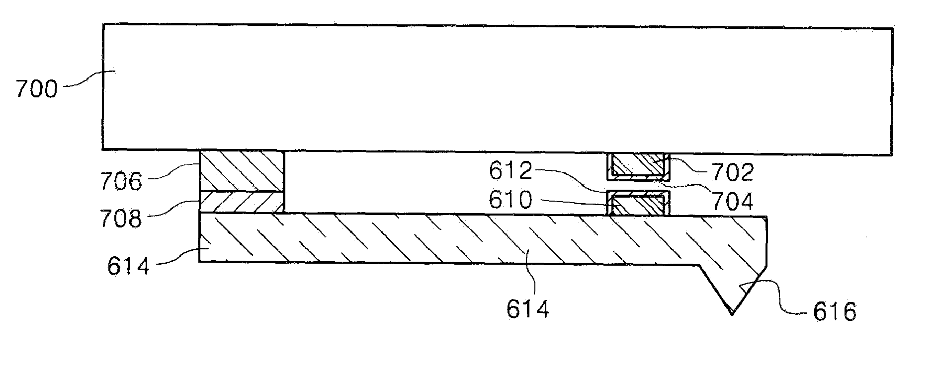
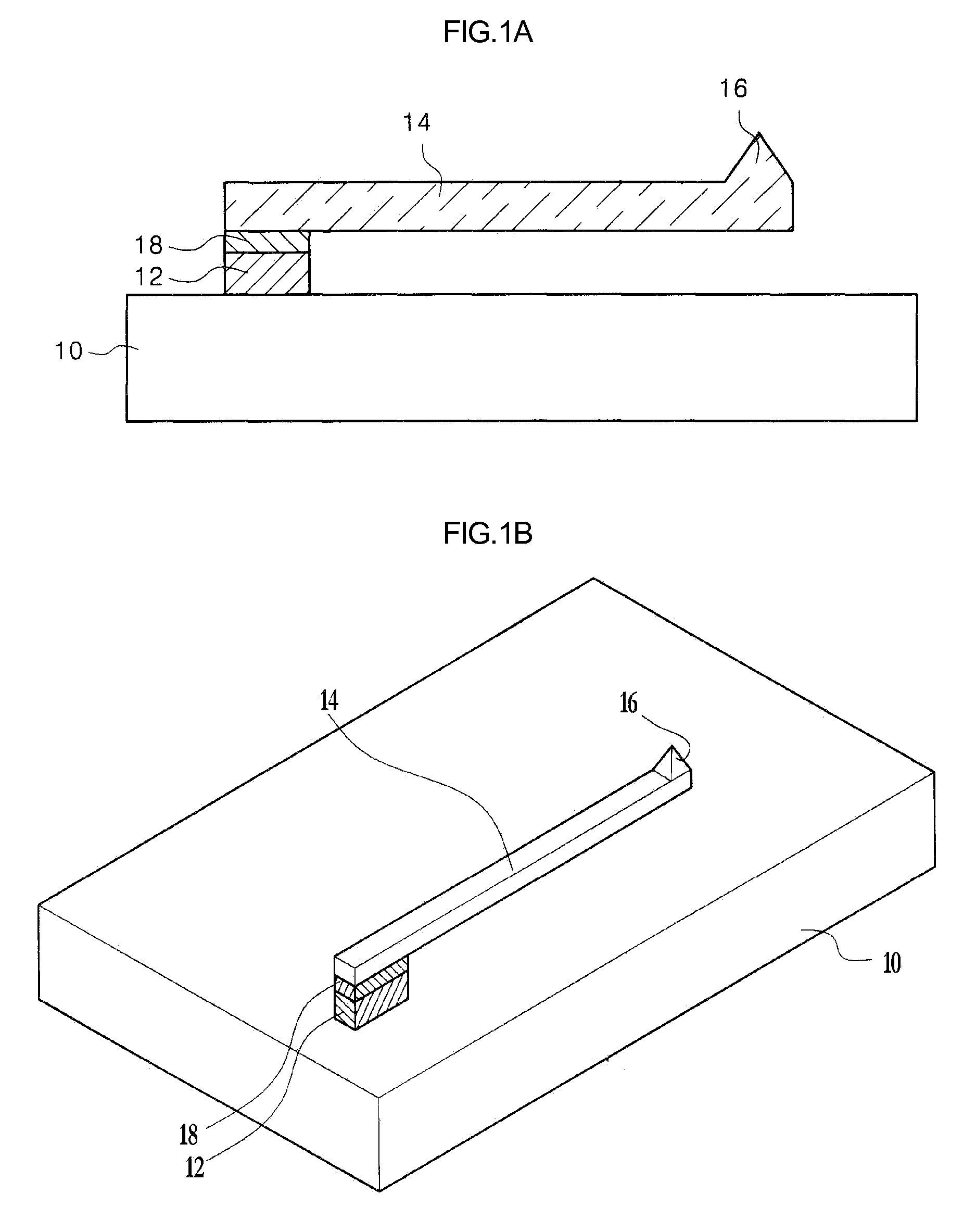
[0084]FIGS. 2 through 10b are cross-sectional views explaining a method for manufacturing an electrical contact element used to test an electronic device, in accordance with the present invention.

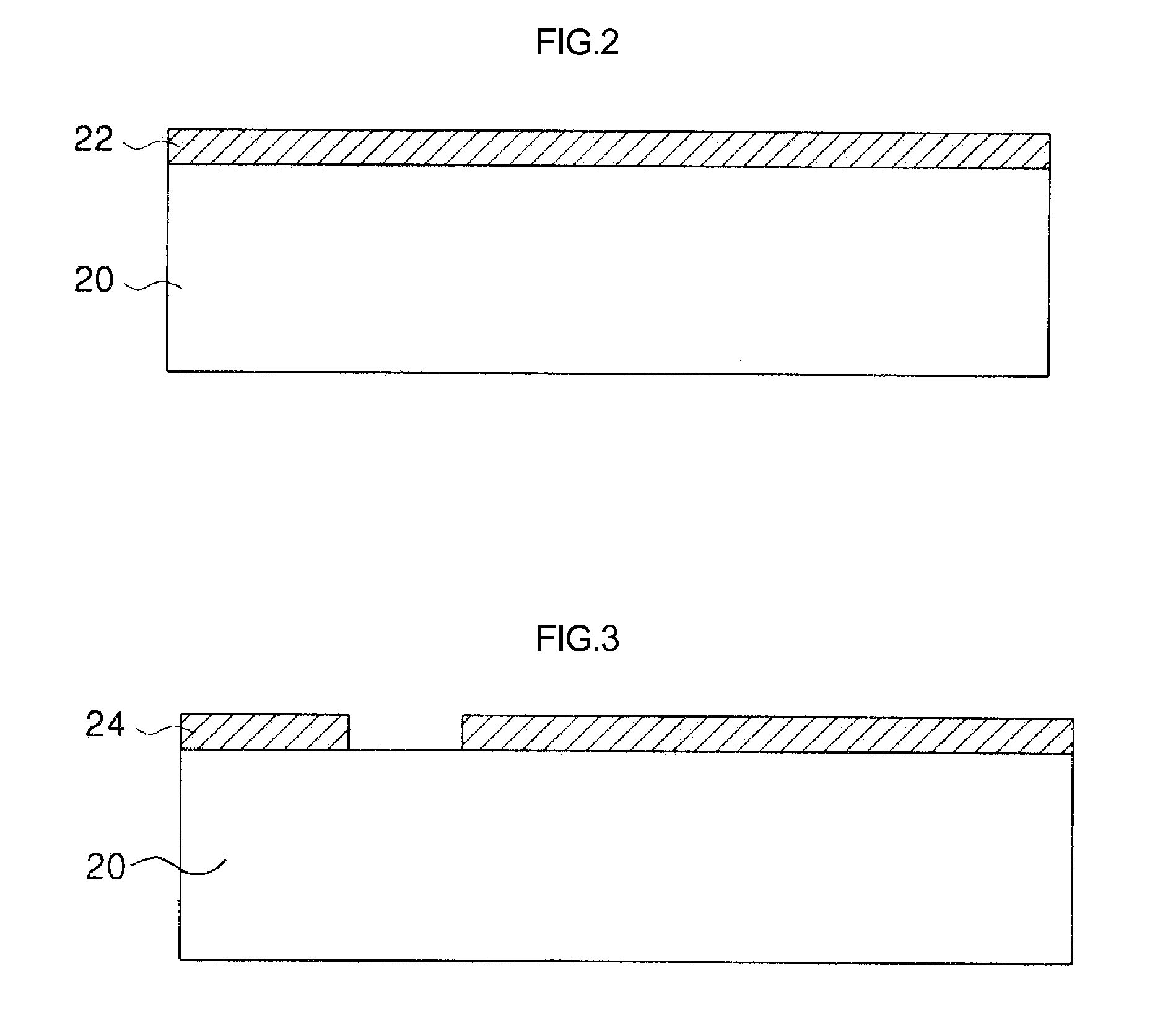
[0085] In the method according to this embodiment of the present invention, first, as shown in FIG. 2, a first protective film 22 of a predetermined thickness is formed on an entire surface of a sacrificial substrate 20 made of silicon having a fixed orientation such as (1 0 0). The first protective film 22 comprises a thin film such as a photoresist and an oxide film. At this time, the photoresist is formed by a spin coating process in which the photoresist is poured onto the sacrificial substrate 20 while the sacrificial substrate 20 is rotated, and the oxide film is formed by the conventional thermal oxidation process.

[0086] Then, as shown in FIG. 3, by implementing a photolithography process which is well known in the art, a first protective film pattern 24 having a first opened region...

second embodiment

[0139] Hereinafter, a method for manufacturing the electrical contact element used to test an electronic device, in accordance with the present invention will be described in detail.

[0140]FIGS. 12 through 18b are cross-sectional views explaining a method for manufacturing an electrical contact element used to test an electronic device, in accordance with a second embodiment of the present invention.

[0141] In the method according to this embodiment of the present invention, first, as shown in FIG. 12, a first protective film of a predetermined thickness is formed on an entire surface of a sacrificial substrate 60 made of silicon having a fixed orientation such as (1 0 0). The first protective film comprises a thin film such as a photoresist and an oxide film. By implementing the same photolithographic process as in the aforementioned first embodiment, a first protective film pattern 62 having a second opened region (not numbered) larger than a first opened region of the first embodi...

third embodiment

[0179]FIGS. 19 through 25b are cross-sectional views explaining a method for manufacturing an electrical contact element used to test an electronic device, in accordance with the present invention.

[0180] In the method according to this embodiment of the present invention, first, as shown in FIG. 19, a first protective film of a predetermined thickness is formed on an entire surface of a sacrificial substrate 80 made of silicon having a fixed orientation such as (1 0 0). The first protective film comprises a thin film such as a photoresist and an oxide film. By implementing the same photolithographic process as in the aforementioned first embodiment, a first protective film pattern 82 having a second opened region (not numbered) larger than the first opened region of the first embodiment is defined.

[0181] Next, by implementing a first etching process using the first protective film pattern 82 as an etching mask, the sacrificial substrate 80 is isotropically etched to define a trench...


PUM


Abstract

Disclosed is an electrical contact element used to test an electronic device. The electrical contact element has a beam portion and a tip portion attached to an end of the beam portion. In representative embodiments, a part of the beam portion is bent, e.g., such that the beam portion is zigzagged one or more times. A projection may be formed around a proximal end of the tip portion.

Description

BACKGROUND OF THE INVENTION [0001] 1. Field of the Invention [0002] The present invention pertains to a method for manufacturing an electrical contact element used to test an electronic device, and an electrical contact element manufactured thereby, and more particularly, the present invention relates to a method for manufacturing an electrical contact element capable of electrically testing an electronic device by being brought into contact with the electronic device to see whether the electronic device is in a normal state or not, and an electrical contact element manufactured thereby. [0003] Further, the present invention relates to a method for manufacturing an electrical contact element capable of electrically testing an electronic device by being increased in its physical force due to the presence of an armrest, to see whether the electronic device is in a normal state or not, and an electrical contact element manufactured thereby. [0004] 2. Description of the Related Art [000...

Claims


Application Information

Patent Timeline
IPC IPC(8): G01R31/02G01R1/067G01R1/073G01R3/00H01L21/66
CPCG01R1/06733G01R1/07342G01R1/06727H05K3/4092G01R3/00
Inventor LEE, OUG-KI
Owner PHICOM CORP
Why Eureka
Try Eureka