Supercharge Your Innovation With Domain-Expert AI Agents!

Program circuit of semiconductor

a technology of programmable memory and semiconductor, applied in the field of programmable memory program circuit of semiconductor onetime, can solve the problems of inability to perform, e.g., remedy, and the downsizing of the fuse cannot keep up with the size of other semiconductor devices, and achieve the effect of stabilizing the element characteristics

Inactive Publication Date: 2006-08-31
KK TOSHIBA
View PDF4 Cites 16 Cited by
  • Summary
  • Abstract
  • Description
  • Claims
  • Application Information

AI Technical Summary

Benefits of technology

[0017] According to an aspect of the present invention, there is provided a semiconductor integrated circuit device comprising a storage element configured to store information by electrically irreversibly changing element characteristics, a program circuit configured to program the storage element by electrically irreversibly changing the element characteristics thereof, the program circuit comprising a high-voltage generator which irreversibly changes the element characteristics of the storage element by applying a high voltage thereto, and a current source which supplies an electric current to the storage element having element characteristics changed by the high-voltage generator, thereby stabilizing the element characteristics, and a sensing circuit configured to sense the irreversibly changed element characteristics of the storage element in distinction from an unchanged state.

Problems solved by technology

The laser fuse stores information by blowing upon being irradiated with a laser beam, thereby causing an irreversible change.
In addition, since the minimum dimension of the laser fuse is determined by the wavelength of the laser beam used, downsizing of the fuse cannot keep step with that of other semiconductor devices.
This makes it impossible to perform, e.g., remedy of defects by a high-speed test after packaging, or built-in self repair using a built-in test circuit of a chip.
Therefore, embedding a nonvolatile memory which stores electric charge in the floating gate requires additional masks and fabrication processes, and increases the fabrication cost.
Consequently, the high voltage VBP is applied to the gate oxide of the MOS transistor MP0 to cause breakdown within a short time.
If, however, the effect of the Joule heat immediately after the breakdown is insufficient, the resistance value rises with time to produce an unstable state, and this may finally make data unreadable and lost.
If the effect of the Joule heat is unsatisfactory, an incomplete breakdown state called soft breakdown occurs, and this may raise the resistance again to make data disappear.
As a consequence, the pattern occupied area of the program circuit, particularly, the charge pump circuit increases in the OTP memory, and this decreases the layout efficiency.

Method used


Image

  • Program circuit of semiconductor
  • Program circuit of semiconductor
  • Program circuit of semiconductor

Examples


Embodiment Construction

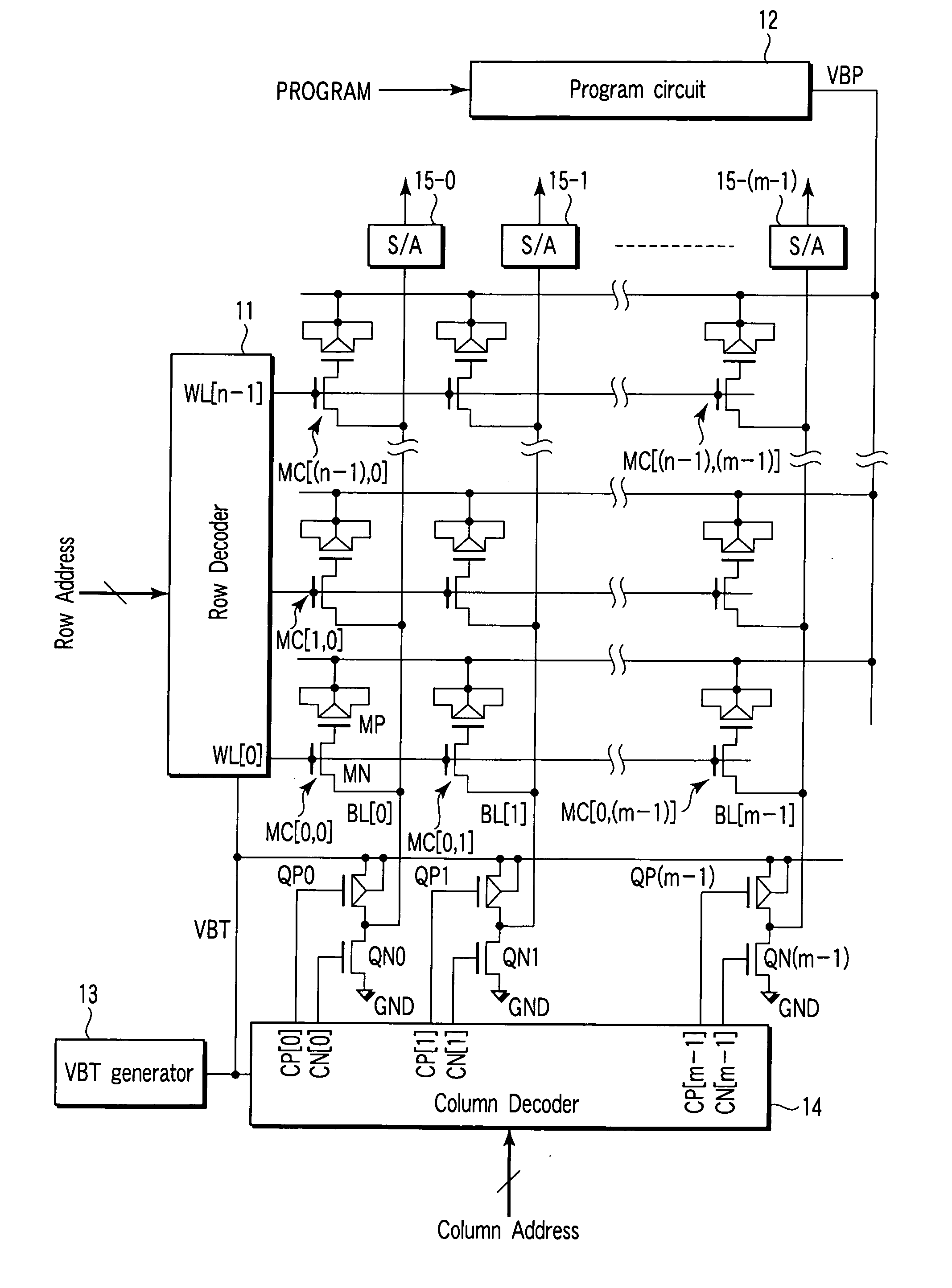
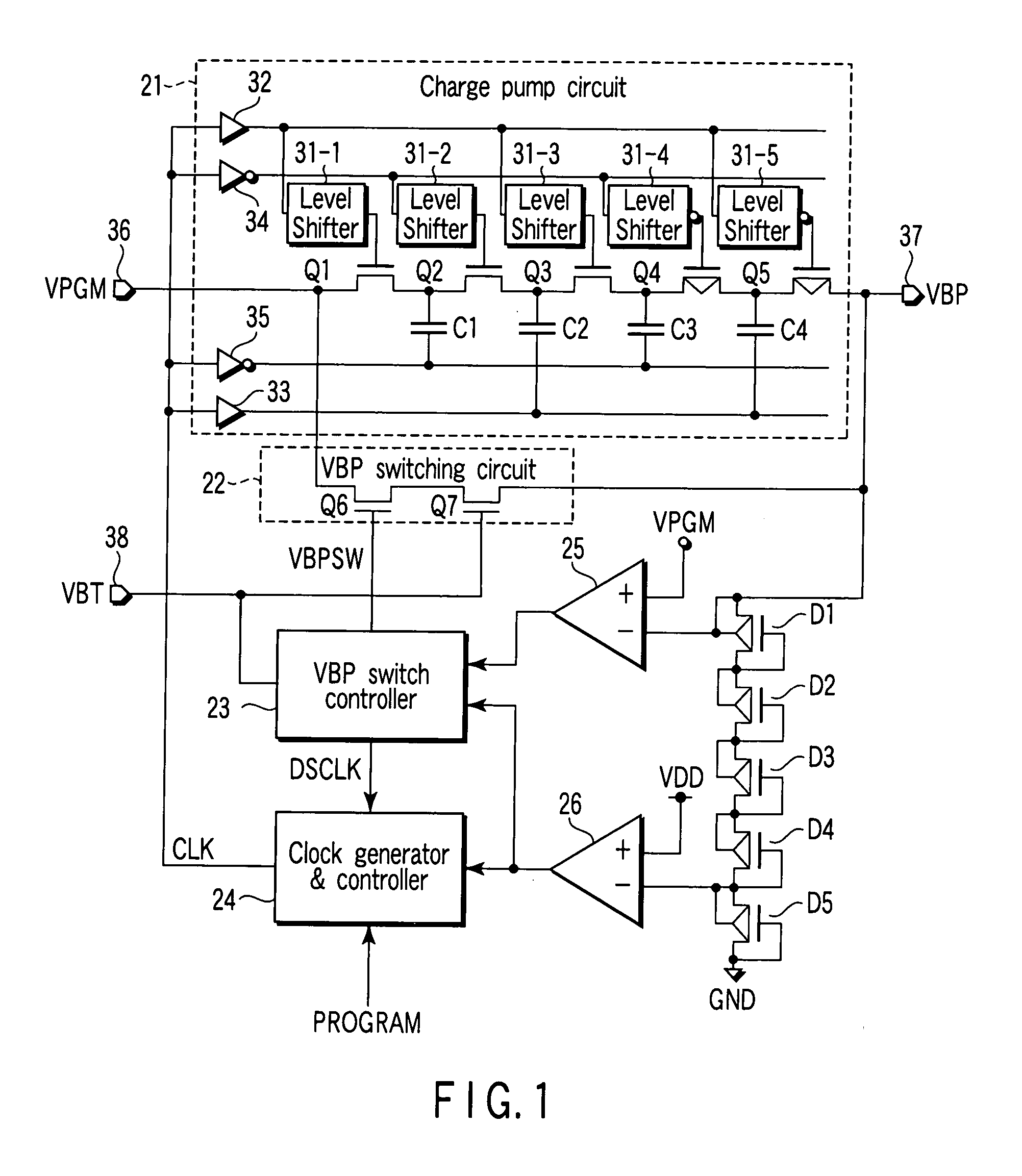
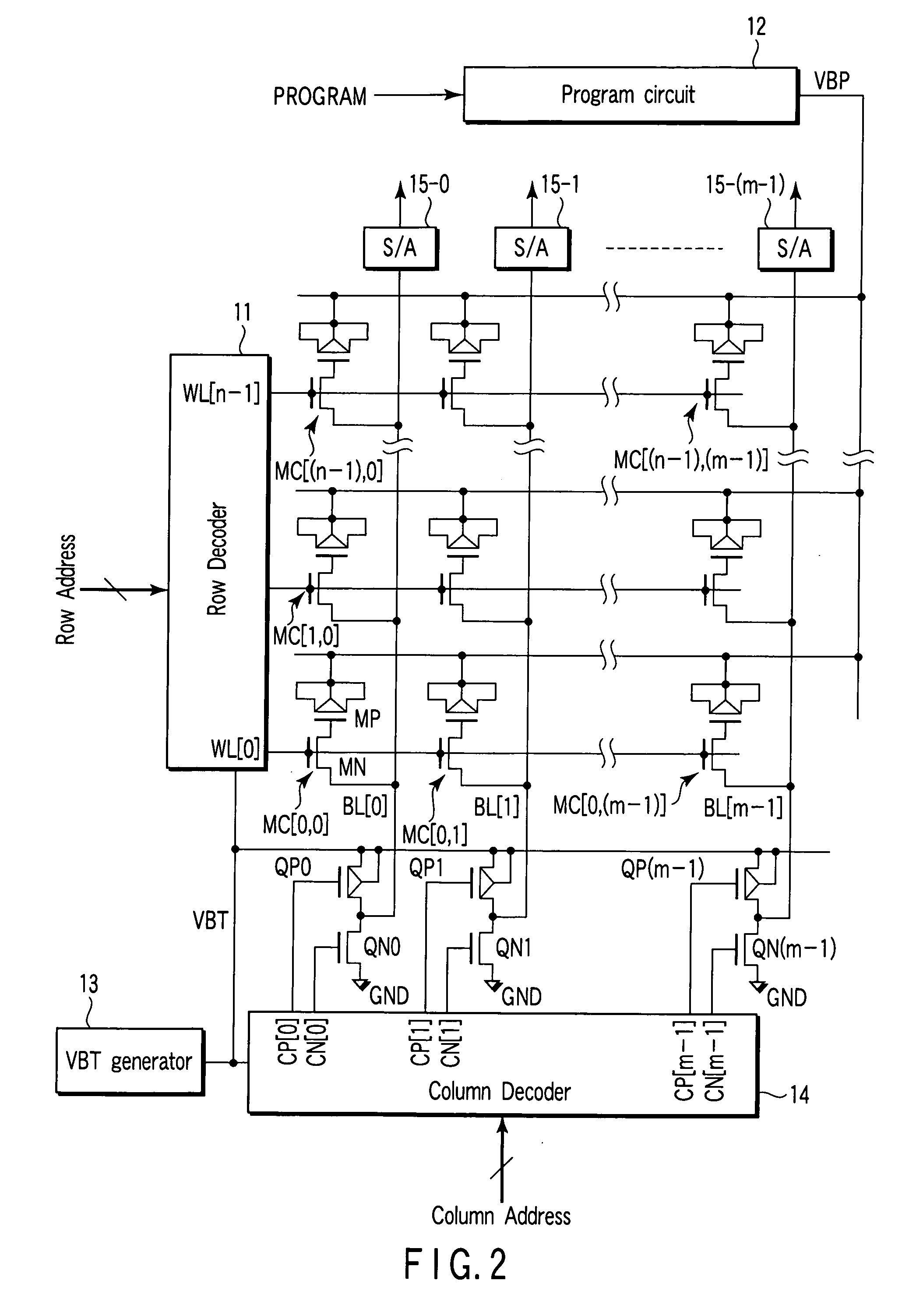
[0020]FIGS. 1 and 2 are views for explaining a semiconductor integrated circuit device according to an embodiment of the present invention. FIG. 1 is a circuit diagram showing a program circuit. FIG. 2 is a circuit diagram showing an outline of the arrangement of a semiconductor one-time programmable memory.

[0021] As shown in FIG. 2, cells MC[0,0] to MC[(n−1),(m−1)] as storage elements are arranged in a matrix. Each of the cells MC[0,0] to MC[(n−1),(m−1)] includes a P-channel MOS transistor MP which functions as an e-fuse, and an N-channel MOS transistor MN. The MOS transistors MN in the cells MC[0,0] to MC[(n−1), (m−1)] have gates connected to word lines WL[0] to WL[n−1] in the individual rows, and sources connected to bit lines BL[0] to BL[m−1] in the individual columns. Each MOS transistor MN functions as both a bit selector and barrier transistor.

[0022] The word lines WL[0] to WL[n−1] are supplied with outputs from a row decoder 11. The row decoder 11 decodes a row address sig...


PUM


Abstract

A semiconductor integrated circuit device includes a storage element, program circuit, and sensing circuit. The storage element stores information by electrically irreversibly changing the element characteristics. The program circuit programs the storage element by electrically irreversibly changing its element characteristics. The sensing circuit senses the irreversibly changed element characteristics of the storage element in distinction from an unchanged state. The program circuit includes a high-voltage generator which irreversibly changes the element characteristics of the storage element by applying a high voltage to it, and a current source which supplies an electric current to the storage element having element characteristics changed by the high-voltage generator, thereby stabilizing the element characteristics.

Description

CROSS-REFERENCE TO RELATED APPLICATIONS [0001] This application is based upon and claims the benefit of priority from prior Japanese Patent Application No. 2005-051807, filed Feb. 25, 2005, the entire contents of which are incorporated herein by reference. BACKGROUND OF THE INVENTION [0002] 1. Field of the Invention [0003] The present invention relates to a semiconductor integrated circuit device including a semiconductor one-time programmable memory using an electrically programmable irreversible storage element and, more particularly, to a program circuit of a semiconductor one-time programmable memory. [0004] 2. Description of the Related Art [0005] In the recent semiconductor integrated circuit devices, a nonvolatile one-time programmable (OTP) memory in which stored data does not disappear even when power supply stops is an essential element. The OTP memory is widely used in, e.g., redundancy of a large-capacity memory such as a DRAM or SRAM, tuning of an analog circuit, storag...

Claims


Application Information

Patent Timeline
IPC IPC(8): G11C11/24
CPCG11C5/145G11C17/16G11C17/18
Inventor ITO, HIROSHI
Owner KK TOSHIBA
Features
  • R&D
  • Intellectual Property
  • Life Sciences
  • Materials
  • Tech Scout
  • Unparalleled Data Quality
  • Higher Quality Content
  • 60% Fewer Hallucinations
Learn More