

Method of processing substrate, and method of and program for manufacturing electronic device
- Summary
- Abstract
- Description
- Claims
- Application Information
AI Technical Summary
Benefits of technology
Problems solved by technology
Method used
Image

Examples
Embodiment Construction
[0060] The present invention will now be described in detail with reference to the drawings showing preferred embodiments thereof.
[0061] First, a method of processing a substrate according to an embodiment of the present invention will be described.
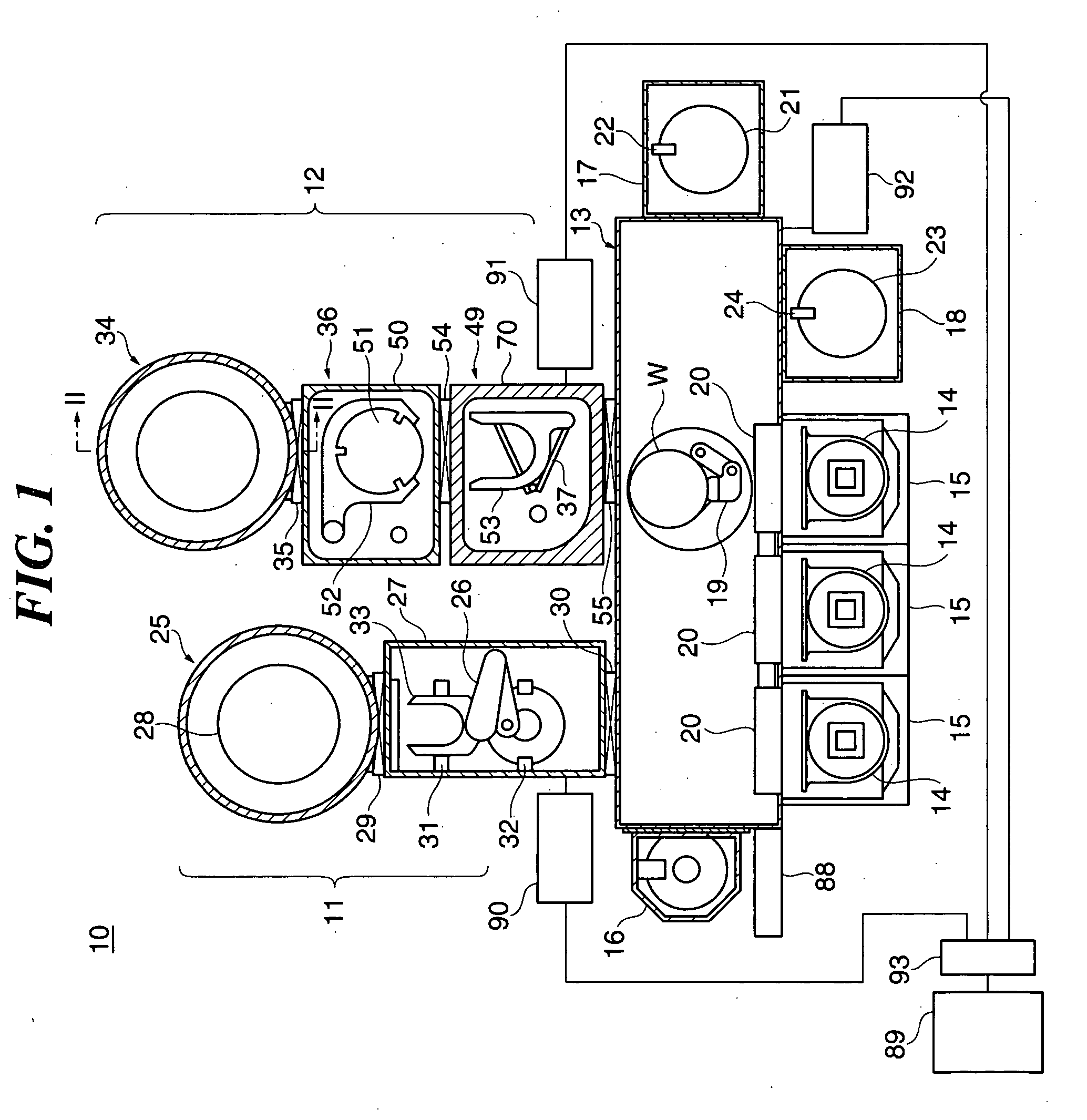
[0062]FIG. 1 is a plan view schematically showing the construction of a substrate processing apparatus to which is applied the method of processing a substrate according to the present embodiment.
[0063] As shown in FIG. 1, the substrate processing apparatus 10 is comprised of a first process ship 11 for carrying out reactive ion etching (hereinafter referred to as “RIE”) on electronic device wafers (hereinafter referred to merely as “wafers”) (substrates) W, a second process ship 12 that is disposed parallel to the first process ship 11 and is for carrying out COR (chemical oxide removal) processing and PHT (post heat treatment) processing, described below, on wafers W that have been subjected to the RIE process in the first process sh...
PUM
| Property | Measurement | Unit |
|---|---|---|
| Temperature | aaaaa | aaaaa |
| Pressure | aaaaa | aaaaa |
| Temperature | aaaaa | aaaaa |
Abstract
Description
Claims
Application Information