Semiconductor device

a memory device and error correction technology, applied in information storage, static storage, digital storage, etc., can solve the problems of increasing power consumption, reducing power consumption, and unable to achieve low power during ordinary operation, and achieve high speed, low voltage operation, and high-integration semiconductor

Inactive Publication Date: 2006-09-07
HITACHI LTD
View PDF10 Cites 21 Cited by
  • Summary
  • Abstract
  • Description
  • Claims
  • Application Information

AI Technical Summary

Benefits of technology

[0011] The main invention disclosed in the present applied specification makes it possible to realize low voltage operati...

Problems solved by technology

Therefore, the mode wherein power consumption can be reduced is limited to the mode wherein only the data storing operation is carried out.
That is, low power cannot be attained during ordinary operation.
Further, when it is attempted to correct an error with an ECC circuit during ordinary operation in such a circuit structure as described in JP-A No. 56671/2002, it is necessary to amplify more I/O lines in comparison with the case where an ECC circuit is not added and t...

Method used


Image

  • Semiconductor device
  • Semiconductor device
  • Semiconductor device

Examples


first embodiment

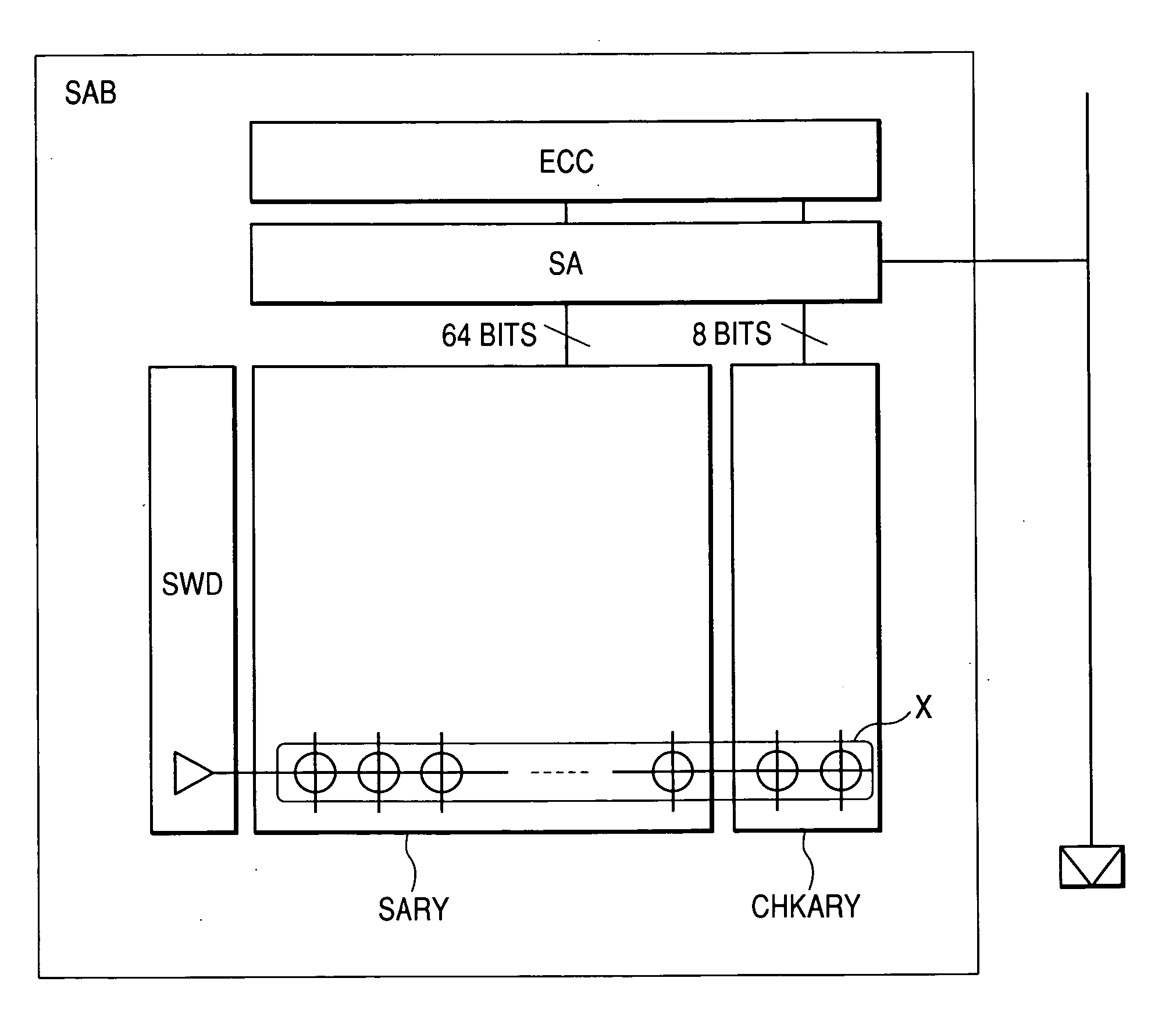
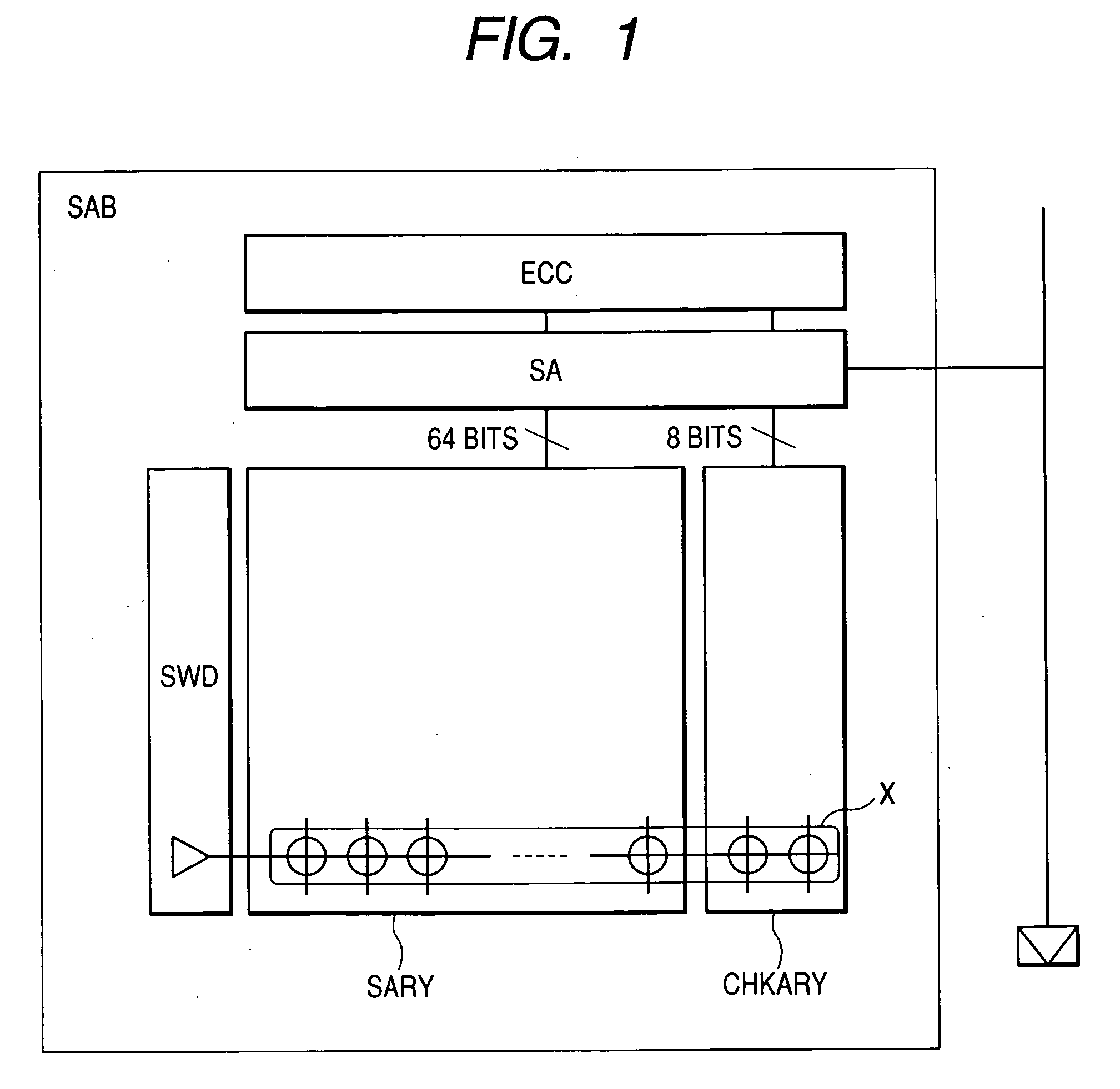
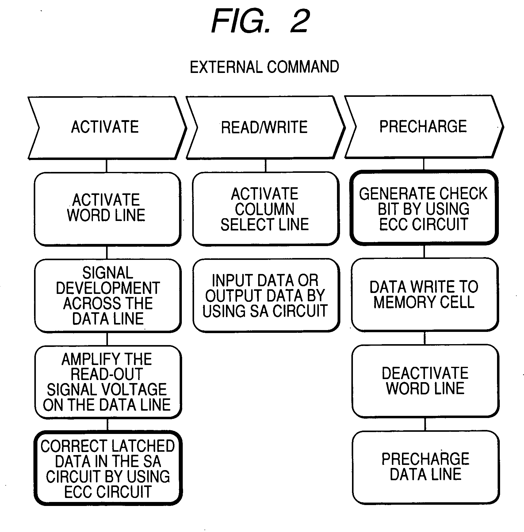
[0034] Firstly, the first embodiment according to the present invention is hereunder explained based on FIGS. 1 to 13. FIG. 1 is a conceptual diagram showing a memory array wherein an error correcting code circuit ECC as the first embodiment according to the present invention is disposed next to a sense amplifier SA, namely for each sub-array block SAB. The reference characters in the figure are as follows: SWD represents a sub-word driver to drive word lines, SARY a memory cell array in which data is stored, CHKARY a check bit array in which information for checking the existence of an error in data in the memory cell array SARY is stored, X a codeword composing one check unit, and ECC one-bit error correcting code circuit to detect and correct an error based on the data and information read out from a memory cell ARY and the check bit array CHKARY. Here, the following embodiments, unless specifically described otherwise, are based on the premise that data is read out in 64 bit uni...

second embodiment

[0049] In the first embodiment, when a readout error is produced, the wrongly readout data is corrected with an error correcting code circuit ECC. However, by means of adding redundant bits and replacing a defective bit with a redundant bit, the voltage can be lowered further than the case of not having redundant bits. As a consequence, a more reliable DRAM array can be realized.

[0050] The check matrix H shown in FIG. 14 is an embodiment of a check matrix wherein redundant bits are added to a sub-array SARY and a check matrix for redundant bits corresponding to the added redundant bits is newly added. As far as an additional check matrix is stored for redundant bits as stated above, even in the case where memory cells connected to the data lines DL8 and DL32 are defective for example, by selecting a matrix of four columns from among the check matrix for redundant bits in order to detect and correct the error on the data line of the replaced redundant bits, even when the data of the...

third embodiment

[0053] In the first and second embodiments, the explanation has been done in the case where a memory cell of a check bit array is not defective. In contrast, when a memory cell of a check bit array has a defective cell capacitor or the like, by preparing beforehand additional plural check bits and a check matrix necessary for the detection and correction of an error in the check bits and using both the check bits and the check matrix for the detecting and correcting operation of the error, it is possible to correct the error data and to realize a highly reliable DRAM array even when a defective cell exists in the check bits and simultaneously an error is produced in the data read out from a sub-array SARY. In other words, even in the case of using a simple hamming code, it becomes possible to correct two bits; one hard error bit in check bits and one soft error bit in the data read out from a sub-array SARY. As a consequence, even when a data line is operated at a low voltage, it is...


PUM


Abstract

When the miniaturization of a DRAM advances, the capacity of a cell capacitor decreases, and further the voltage of a data line is lowered, the amount of read signals remarkably lowers, errors are produced during readout, and the yield of chips lowers. To solve the above problems, the present invention provides a DRAM that: has an error correcting code circuit for each sub-array; detects and corrects errors with said error correcting code circuit in both the reading and writing operations; and further has rescue circuits in addition to said error correcting code circuits and replaces a defective cell caused by hard error with a redundant bit.

Description

CLAIM OF PRIORITY [0001] The present application claims priority from Japanese application JP 2005-055294 filed on Mar. 1, 2005, the content of which is hereby incorporated by reference into this application. FIELD OF THE INVENTION [0002] The present invention relates to a semiconductor device and more particularly to an error correcting code circuit of a low-power high-speed semiconductor memory device. BACKGROUND OF THE INVENTION [0003] Dynamic random access memories (hereunder referred to as “DRAM”), a kind of semiconductor memory devices, are mounted in quantity on various electric devices, which we usually use, as main memories of large-scale computers and personal computers and work memories of digital appliances such as mobile phones, digital cameras and the like. Then in accordance with the recent needs for the devices having lower power consumption and higher performances, DRAMs to be mounted on the devices are also required to have higher performances including a lower pow...

Claims


Application Information

Patent Timeline
IPC IPC(8): G11C29/00
CPCG11C11/401G11C29/42G11C29/44G11C29/4401
Inventor AKIYAMA, SATORUTAKEMURA, RIICHIROSEKIGUCHI, TOMONORI
Owner HITACHI LTD
Why Eureka
Try Eureka