Semiconductor devices integrating high-voltage and low-voltage field effect transistors on the same wafer

a field effect transistor and high-voltage technology, applied in the direction of semiconductor devices, transistors, electrical equipment, etc., can solve the problems of reducing the maximum output current, the maximum output power, and the deterioration of high frequency performance, and achieve high reliability and high breakdown voltage.

Inactive Publication Date: 2006-09-14
WIN SEMICON
View PDF2 Cites 16 Cited by
  • Summary
  • Abstract
  • Description
  • Claims
  • Application Information

AI Technical Summary

Benefits of technology

[0009] Accordingly, it is an object of the present invention to provide a novel field-plate structure for a Schottky gate FET, which not only makes the device to have a hi

Problems solved by technology

Such a large electric field will lead to an avalanche breakdown in the channel region between the gate and the drain electrodes, resulting in a deterioration of high frequency performance.
However, larger gate-drain distance will also lead to larger sheet resistance, which in effect reduces the maximum output current and hence the maximum output power that could be extracting from the device.
However, it is

Method used


Image

  • Semiconductor devices integrating high-voltage and low-voltage field effect transistors on the same wafer
  • Semiconductor devices integrating high-voltage and low-voltage field effect transistors on the same wafer
  • Semiconductor devices integrating high-voltage and low-voltage field effect transistors on the same wafer

Examples


Embodiment Construction

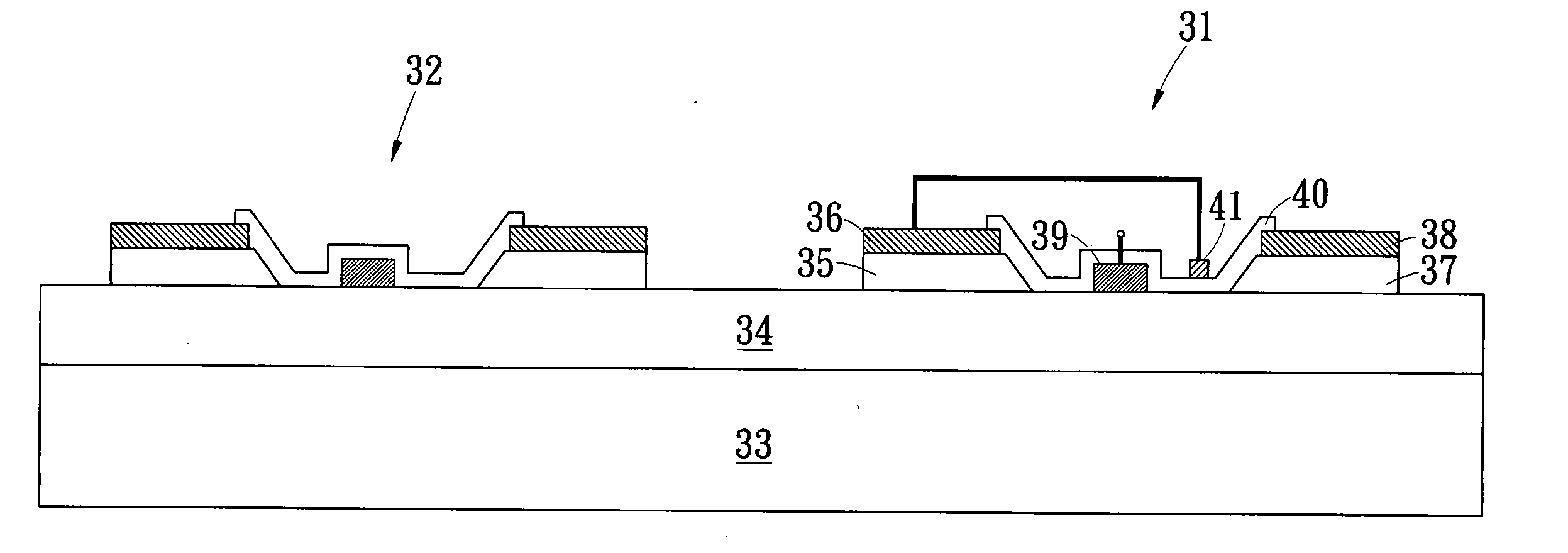
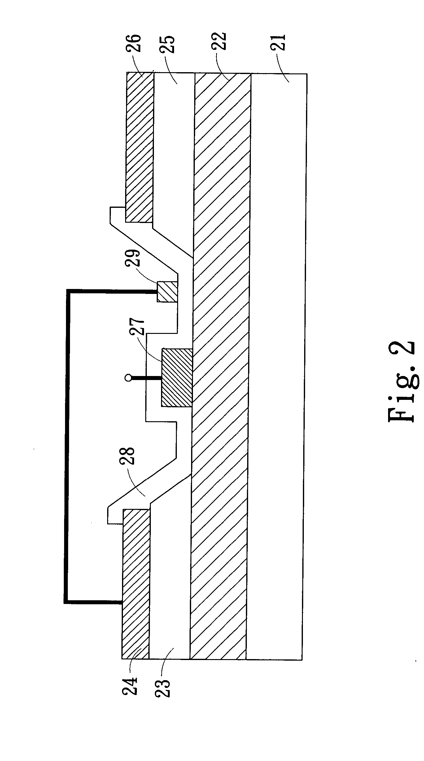
[0018]FIG. 2 is a cross-section view of the Schottky gate FET structure of the present invention having a separated field plate thereon. The semiconductor layer structure in FIG. 2 generally comprises a substrate 21 and a channel layer 22 thereon, whereon a contact layer is formed. The contact layer has a source region 23, a drain region 25 with a distance apart from the source region 23 and a recess region being formed by removing part of the contact layer between the source region 23 and the drain region 25. A source electrode 24 and a drain electrode 26 are formed on the source region 23 and the drain region 25, respectively. Both the source electrode 24 and the drain electrode 26 make an ohmic contact with the contact layer, and being electrically coupled to the channel layer 22 underneath. On the recess region of the contact layer, a gate electrode 27, having a finger shape, is formed and making a Schottky contact with the channel layer 22 underneath. After the formation of the...


PUM


Abstract

A field effect transistor (FET) with novel field-plate structure relates to a Schottky gate FET structure with field plate thereon for high voltage operations. The structure and fabrication processes thereof not only provide a reliable way to produce high-voltage FETs, but also allow the integration of conventional low-voltage FETs on the same wafer.

Description

FIELD OF THE INVENTION [0001] The present invention generally relates to a semiconductor device. More specifically, the present invention relates to a field-effect transistor (FETs) having a novel field plate structure thereon, which involves fabrication processes that are fully compatible with those of conventional low-voltage FETs and are capable of integrating high-voltage and low-voltage FETs on the same wafer. BACKGROUND OF THE INVENTION [0002] Compound semiconductor field effect transistor (FET) operating at microwave frequency is the key component used in wireless and satellite communications. Well known devices for such applications include GaAs metal-semiconductor FETs (MESFETs) and Heterostructure FETs, such as AlGaAs / GaAs based high electron mobility transistor (HEMT) as well as pseudomorphic HEMT (PHEMT) with strained channel layer therein. [0003] For a conventional FET, it generally comprises a Schottky gate electrode thereon and a source and a drain electrodes being oh...

Claims


Application Information

Patent Timeline
IPC IPC(8): H01L29/00
CPCH01L27/095H01L29/402H01L29/812
Inventor CHERTOUK, MOURAD
Owner WIN SEMICON
Why Eureka
Try Eureka