Plasma igniting method and substrate processing method

a substrate processing and igniting technology, applied in the direction of electrical devices, electrical discharge tubes, decorative arts, etc., can solve the problems of increased gate leakage current, low temperature oxide film formation, and insufficient base oxide film of high-k dielectric oxide film

Active Publication Date: 2006-09-14
TOKYO ELECTRON LTD
View PDF10 Cites 12 Cited by
  • Summary
  • Abstract
  • Description
  • Claims
  • Application Information

AI Technical Summary

Benefits of technology

[0021] It is a more specific object of the present invention to provide a plasma igniting method capable of realizing an efficient plasma ignition and a substrate processing method using such a plasma igniting method.
[0045] In accordance with the present invention, in a plasma igniting method for igniting a plasma inside a plasma source provided for a processing container and a substrate processing method using such a plasma igniting method, by flowing a gas containing oxygen in the processing container, irradiating, in the processing container, an ultraviolet light to the gas containing oxygen while pumping the inside of the processing container, and driving the plasma source, a plasma ignition becomes easy as moisture attached to the inner wall of the processing container is separated.
[0047] wherein, before the step of supplying the processing gas carried out after the step of forming the plasma, by including the step of removing the processing gas from a line supplying the processing gas to the plasma source, and further, by executing the step of supplying the processing gas so as to gradually increase a flow rate of the processing gas to a predetermined flow rate, and further, at that time, by executing the step of supplying the processing gas such that the substrate is rotated at least once before the flow rate of the processing gas reaches the predetermined flow rate, an overshoot problem of a processing gas flow rate, occurring at the beginning of the gas supply, is solved, and it also becomes possible to form a uniform film on the entire surface of the substrate.

Problems solved by technology

In such an extremely thin gate insulating film, a tunneling current is increased, which in turn inevitably increases a gate leakage current.
However, such a thermal oxide film formed at a low temperature is liable to include defects such as interface states or the like, and inadequate for the base oxide film of the high-K dielectric oxide film.
However, in such a substrate processing apparatus 20, it has been found that a plasma cannot be easily ignited when the operation is restarted after the processing container 21 has not been operated while the processing container 21 has been left under a vacuum condition for 2˜3 days or longer, or has been open to atmosphere for a maintenance and / or the repair.
However, such a purge process over a long period of time deteriorates the substrate processing efficiency significantly.

Method used


Image

  • Plasma igniting method and substrate processing method
  • Plasma igniting method and substrate processing method
  • Plasma igniting method and substrate processing method

Examples


first preferred embodiment

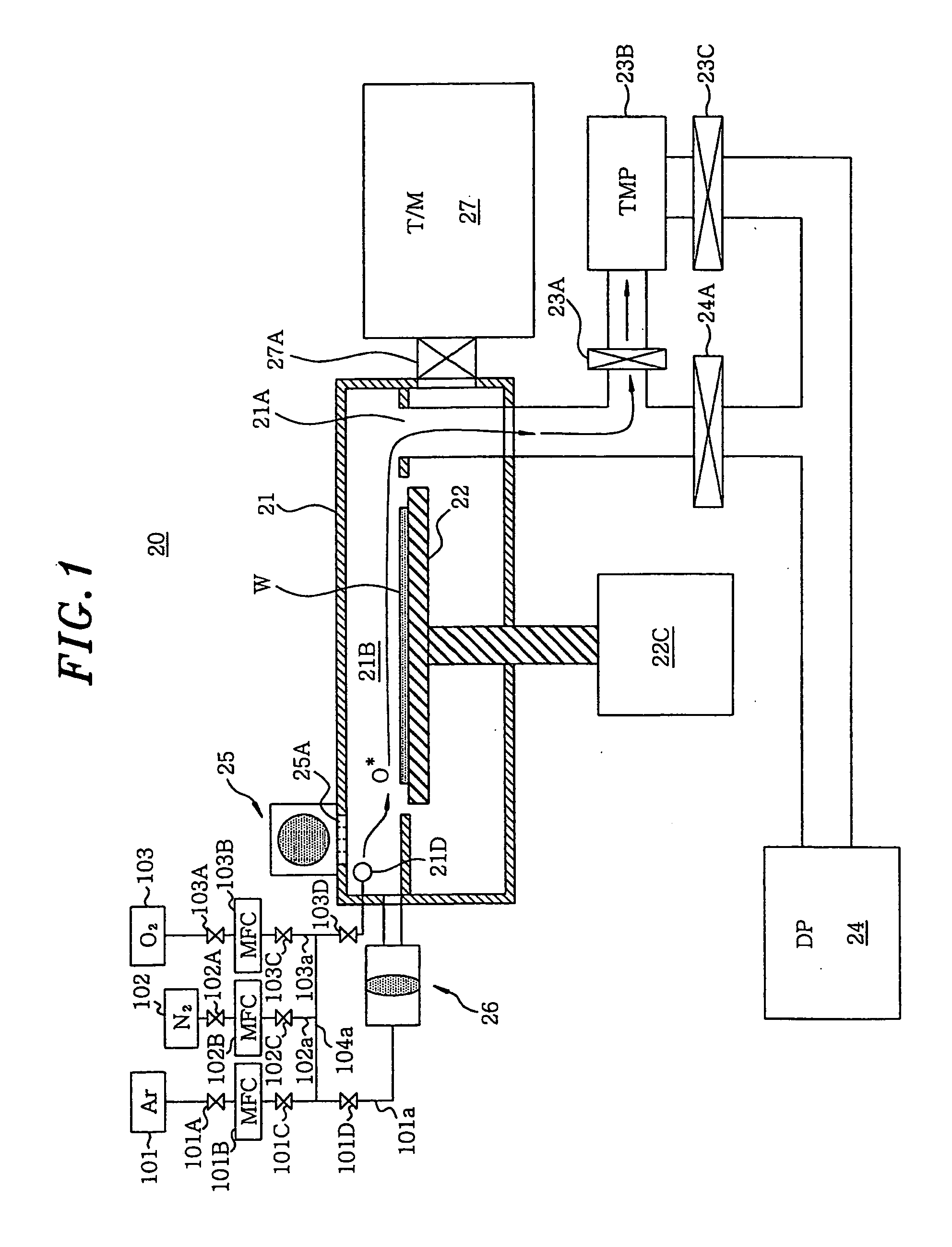
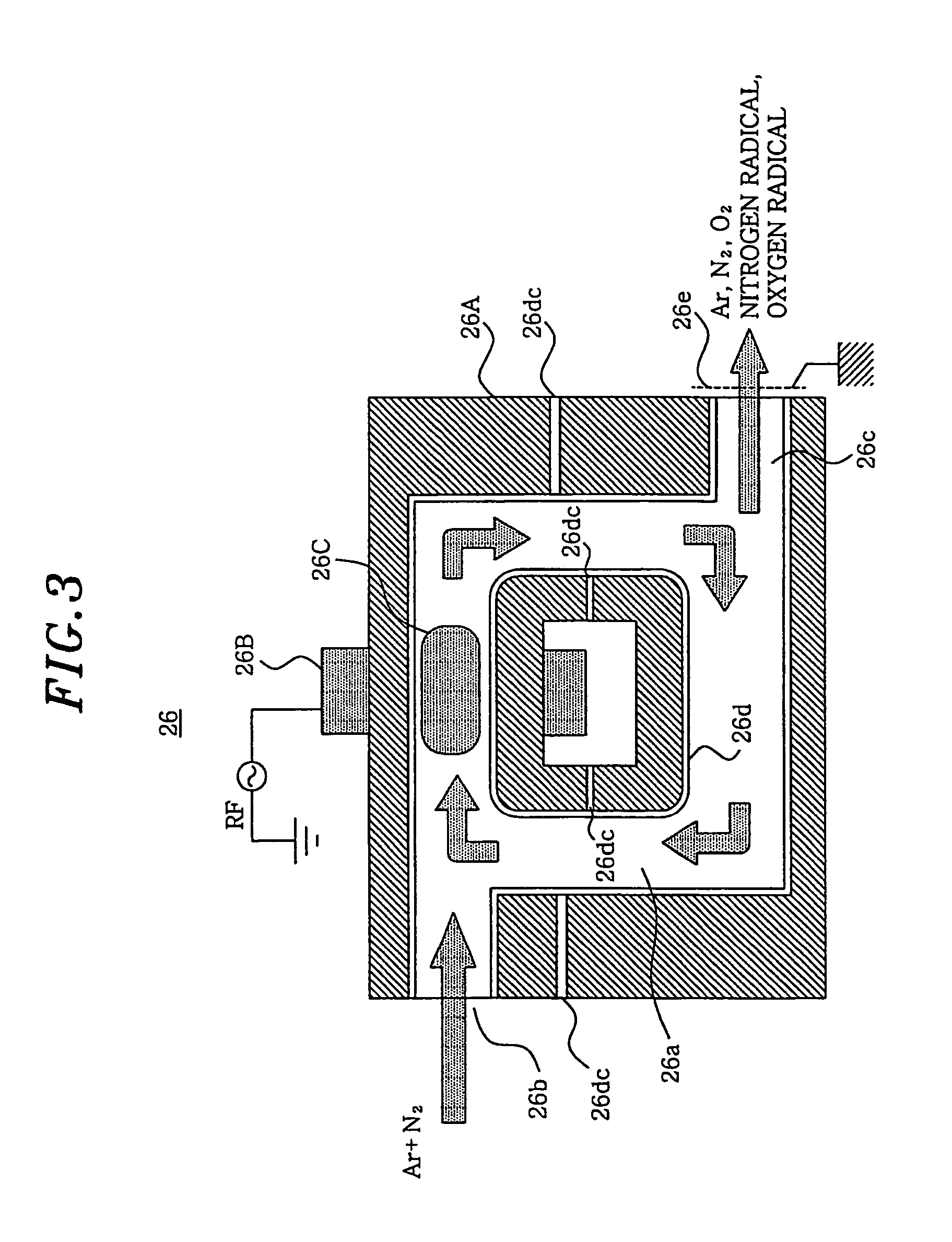
[0064]FIG. 3 presents a configuration view of a high frequency plasma source used in the substrate processing apparatus 20 shown in FIG. 1, as the remote plasma source 26.

[0065] Referring to FIG. 3, the remote plasma source 26 includes a block 26A typically formed of aluminum, in which a gas circulation passage 26a is formed together with a gas inlet 26b and a gas outlet 26c communicating therewith, and there is formed a ferrite core 26B on a part of the block 26A. Further, there is formed a DC blocking insulator 26dc on a part of the block 26A.

[0066] There is provided an alumite film 26d on inner surfaces of the gas circulating passage 26a, the gas inlet 26b and the gas outlet 26c, and further, the alumite film 26d is impregnated with a fluorocarbon resin. A plasma 26C is formed in the gas circulation passage 26a by perpendicularly supplying a high-frequency (RF) power of 400 kHz frequency to a coil wound around the ferrite core 26B.

[0067] By the excitation of the plasma 26C, ni...

second preferred embodiment

[0090] However, in step 5 or step 14 of the above preferred embodiment, in case of igniting a plasma by driving the remote plasma source 26, the ignition condition is substantially limited, and the plasma is not ignited easily if an Ar gas and a processing gas, that is, a nitrogen gas are supplied at the same time.

[0091]FIG. 7 presents a gas supply sequence of such a remote plasma source 26.

[0092] Referring to FIG. 7, an Ar gas is supplied to the remote plasma source 26 at time t1, and a high frequency power is supplied at time t2, and thus, the plasma is ignited. Further, in the sequence of FIG. 7, the supply of a nitrogen gas is started at time t3. At that time, the flow rate of the nitrogen gas supplied by a mass flow rate controller is increased slowly so that the plasma is sustained with stability.

[0093] However, practically, in case of starting the supply of a nitrogen gas at time t3, a large amount of nitrogen gas is supplied in a moment, thus an overshoot of a nitrogen fl...

third preferred embodiment

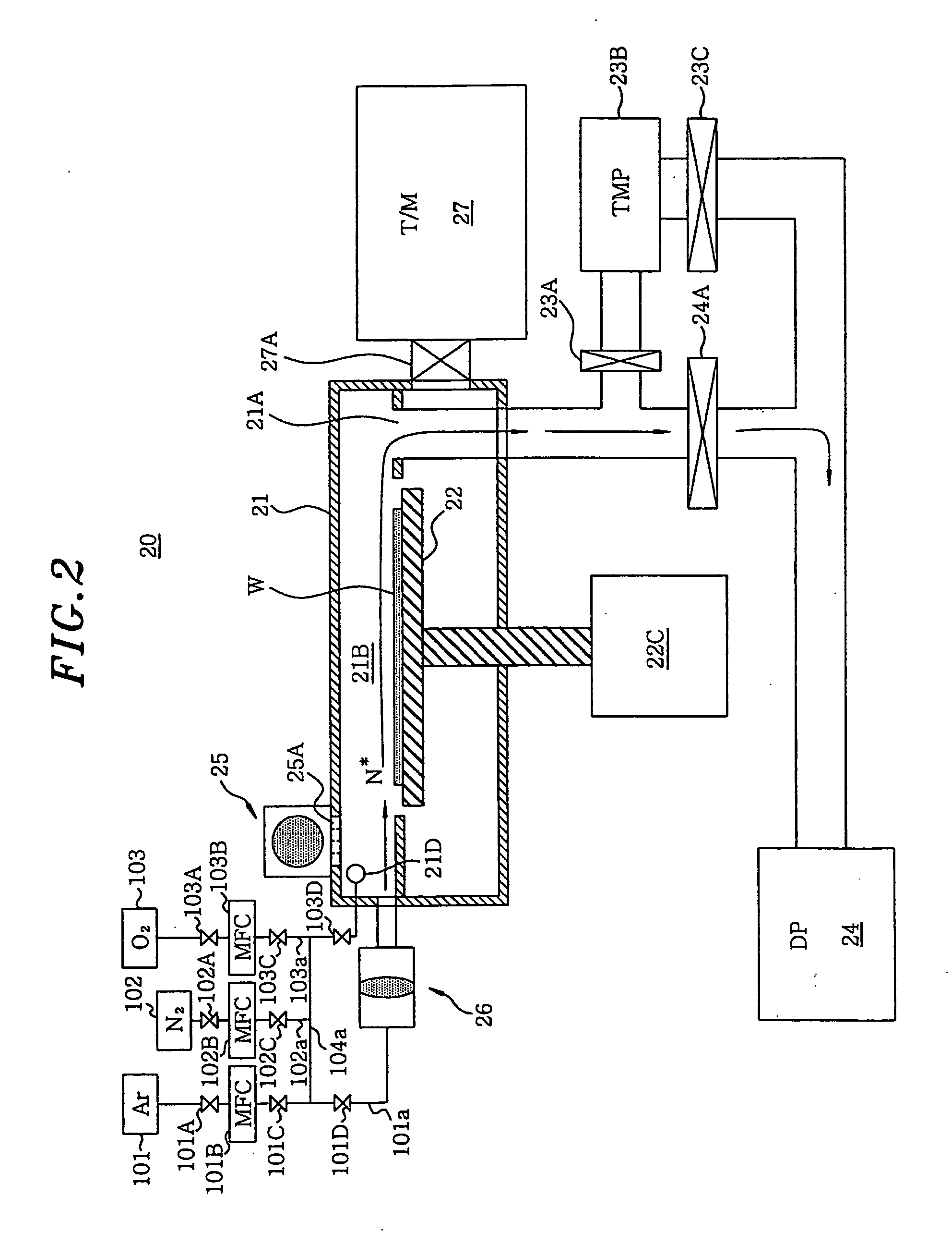
[0102] As explained above, when the UVO2 processing is executed, in the substrate processing apparatus 20 shown in FIG. 1, the moisture is separated from the inner wall of the processing container 21, and thus, the concentration of residual H2O is increased in the process space 21B. Similarly, the moisture is also separated in case of executing a UVNO processing including the steps of: introducing a NO gas through the nozzle 21D; by exciting it with the ultraviolet light source 25, forming nitrogen radicals N and oxygen radicals O*; and forming SiON film on the silicon substrate surface by using thus formed nitrogen radicals N* and oxygen radicals O* in the substrate processing apparatus 20 shown in FIG. 1.

[0103] In case of the above UVO2 processing, when nitriding the silicon oxide film formed by the UVO2 processing by generating an Ar / N2 plasma by the remote plasma source 26 by the RFN processing, the concentration of the residual H2O in the process space 21B is rapidly decreased...


PUM

PropertyMeasurementUnit
Partial pressureaaaaaaaaaa
Pressureaaaaaaaaaa
Wavelengthaaaaaaaaaa

Abstract

A method to solve such a problem that plasma will not ignite in restarting operation of a processing container that has not been operated with the inside kept drawn to vacuum. Gas containing oxygen is passed in a processing container 21, and ultraviolet light is irradiated to the gas while gas inside the processing container 21 is being discharged. After that, a remote plasma source 26 is driven to ignite plasma.

Description

[0001] This application is a Continuation Application of PCT International Application No. PCT / JP2004 / 016588 filed on Nov. 9, 2004, which designated the United States.FIELD OF THE INVENTION [0002] The present invention relates to a manufacture of a semiconductor apparatus; more particularly, to a substrate processing apparatus using oxygen radicals and nitrogen radicals. BACKGROUND OF THE INVENTION [0003] Due to the recent progress in miniaturization processes, the technology in the regime of a gate length of 0.1 μm or less is on the verge of being available for a real application in an ultrahigh speed semiconductor device. In general, while an operating speed of a semiconductor device is improved by miniaturization, accompanied with the reduction of the gate length achieved as a result of the device miniaturization in such an extremely miniaturized semiconductor device, it is imperative to reduce the thickness of a gate insulating film as well in accordance with a scaling rule. [00...

Claims


Application Information

Patent Timeline
IPC IPC(8): C23F1/00H01L21/20H01J37/32H01L21/316
CPCH01J37/32009H01L21/0214H01L21/02238H01L21/02249H01L21/02332H01L21/0234H01L21/31662H01L21/3065
Inventor IGETA, MASANOBUYAMAZAKI, KAZUYOSHIAOYAMA, SHINTAROSHINRIKI, HIROSHI
Owner TOKYO ELECTRON LTD
Why Eureka
Try Eureka