Processor/memory module with foldable substrate

a technology of memory module and processor, applied in the association of printed circuit non-printed electric components, semiconductor/solid-state device details, instruments, etc., can solve the problems of limiting the extent to which multiple integrated circuits can be laterally interconnected, increasing the signal propagation delay, and bulky packaging schemes. , to achieve the effect of saving spa

Inactive Publication Date: 2006-09-21
MOSHAYEDI MARK
View PDF16 Cites 11 Cited by
  • Summary
  • Abstract
  • Description
  • Claims
  • Application Information

AI Technical Summary

Benefits of technology

[0013] The invention relates to packaging a processor and its associated memory onto a subassembly, which mounts onto a main printed circuit board. The subassembly saves space on the main printed circuit board.

Problems solved by technology

As the size and complexity of semiconductors increases, packaging schemes have become bulky in providing routing channels for the high number of signals that are routed from the integrated circuit to the package pins.
The desire to provide the capability of integrated circuits to be used in relatively small devices limits the extent to which multiple integrated circuits can be laterally interconnected while still fitting within the device.
Lateral extension and interconnection of semiconductor devices tends to lead to relatively long interconnects or traces between devices which increases the signal propagation delay, and thus, decreases the circuit operating speed.
Further, lengthy traces increase both the radio-frequency interference (RFI) and electromagnetic interference (EMI) emitted from the printed circuit board.
However, the semiconductors forming the subassembly generate heat, which is often difficult to remove from the densely populated and compact subassembly.
If the excess heat is not removed from the subassembly, the semiconductors may not function properly and may ultimately fail.
Further, it is often difficult to test some pins or interconnect nodes on the densely populated subassembly because the pins or interconnect nodes are buried in the folded subassembly.
It may also not be possible to access the pins with test equipment.
Even if the nodes are not buried, the probes on the test equipment may be too large or bulky to adequately reach areas on the subassembly.

Method used


Image

  • Processor/memory module with foldable substrate
  • Processor/memory module with foldable substrate
  • Processor/memory module with foldable substrate

Examples


Embodiment Construction

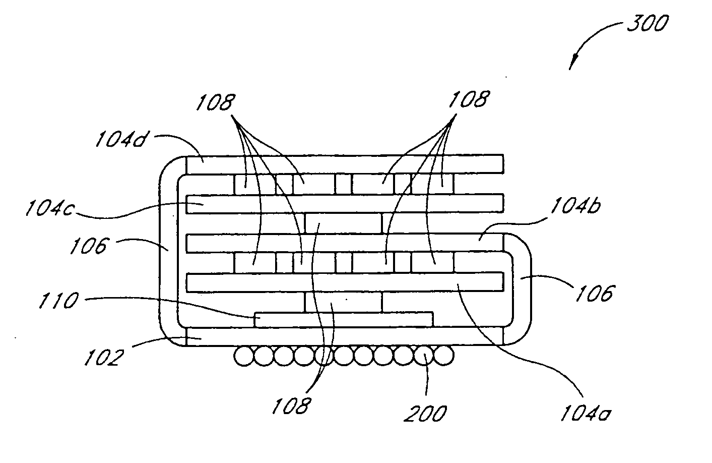
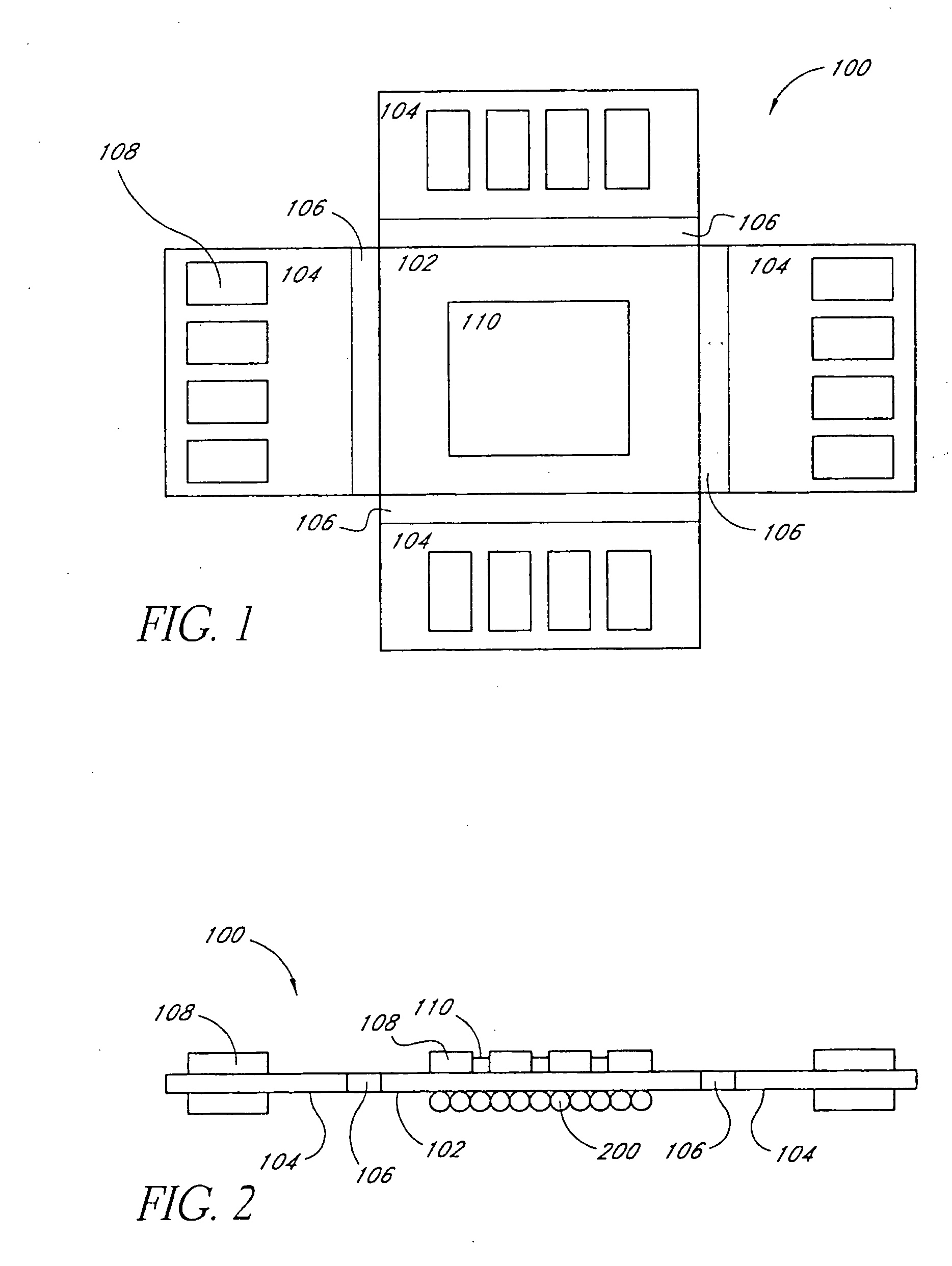
[0036] For a more detailed understanding of the invention, reference is first made to FIG. 1. FIG. 1 illustrates an embodiment of a semiconductor subassembly 100 for packaging a plurality of semiconductor components. The subassembly 100 comprises a substrate with a center section 102 and appendages or wings 104. The center section 102 forms the central structure or board for supporting the foldable appendages or wings 104.

[0037] In this example, the subassembly 100 has four wings for illustrative purposes only. In other embodiments, the subassembly 100 can have less than four wings 104 or more than four wings 104. It is understood that the number of appendages or wings 104 is not limited to four and the apparatus and methods described below apply to subassemblies 100 with more or less than four appendages 104.

[0038] In the illustrated example of FIG. 1, the center section 102 provides a perimeter for attaching the appendages 104. A first appendage 104 has a first end that connects...


PUM


Abstract

A packaging approach reduces the overall footprint for interconnecting multiple semiconductor devices. In an embodiment, a processor mounts onto the center of a substrate with flexible appendages and memory components mount to the flexible appendages. The appendages fold over the processor to produce a processor/memory module. The processor/memory module occupies less area on the main printed circuit board than the laterally interconnected processor and memory devices would occupy.

Description

CROSS-REFERENCE TO RELATED APPLICATIONS [0001] This application is a continuation of U.S. patent application Ser. No. 10 / 845,373 filed May 13, 2004, entitled “PROCESSOR / MEMORY MODULE WITH FOLDABLE SUBSTRATE,” which is hereby incorporated by reference and which claims the benefit of U.S. Provisional Application No. 60 / 471,544, filed May 19, 2003, entitled “PROCESSOR / MEMORY MODULE WITH FOLDABLE SUBSTRATE”, the entirety of which is hereby incorporated herein by reference.BACKGROUND [0002] 1. Field of Invention [0003] The invention relates to increasing the density of integrated circuits on a printed circuit board, and more particularly, to increasing the density of memory associated with a processor on a printed circuit board. [0004] 2. Description of Related Art [0005] Modern electronic devices, such as computers and the like, typically include semiconductor devices, such as integrated circuits. Integrated circuits are microcircuits formed on a semiconductor substrate and packaged in ...

Claims


Application Information

Patent Timeline
Patent Type & Authority Applications(United States)
IPC IPC(8): H05K7/20G11C5/00H01L23/31H01L23/367H01L23/538H05K1/18
CPCH01L23/3114H01L23/3675H01L23/5387H01L2924/3011H01L2924/3025H05K1/189H01L2924/0002H01L2924/00
Inventor MOSHAYEDI, MARK
Owner MOSHAYEDI MARK
Why Eureka
Try Eureka