Ohmic electrode structure, compound semiconductor light emitting device having the same and led lamp
a technology of compound semiconductor and light-emitting device, which is applied in the manufacture of semiconductor/solid-state devices, semiconductor devices, electrical devices, etc., can solve the problems of high forward voltage (vf), high input resistance, and failure to achieve the formation of an ohmic electrode exhibiting excellent ohmic contact properties with respect to p-type boron phosphid
- Summary
- Abstract
- Description
- Claims
- Application Information
AI Technical Summary
Benefits of technology
Problems solved by technology
Method used
Image
Examples
example 1
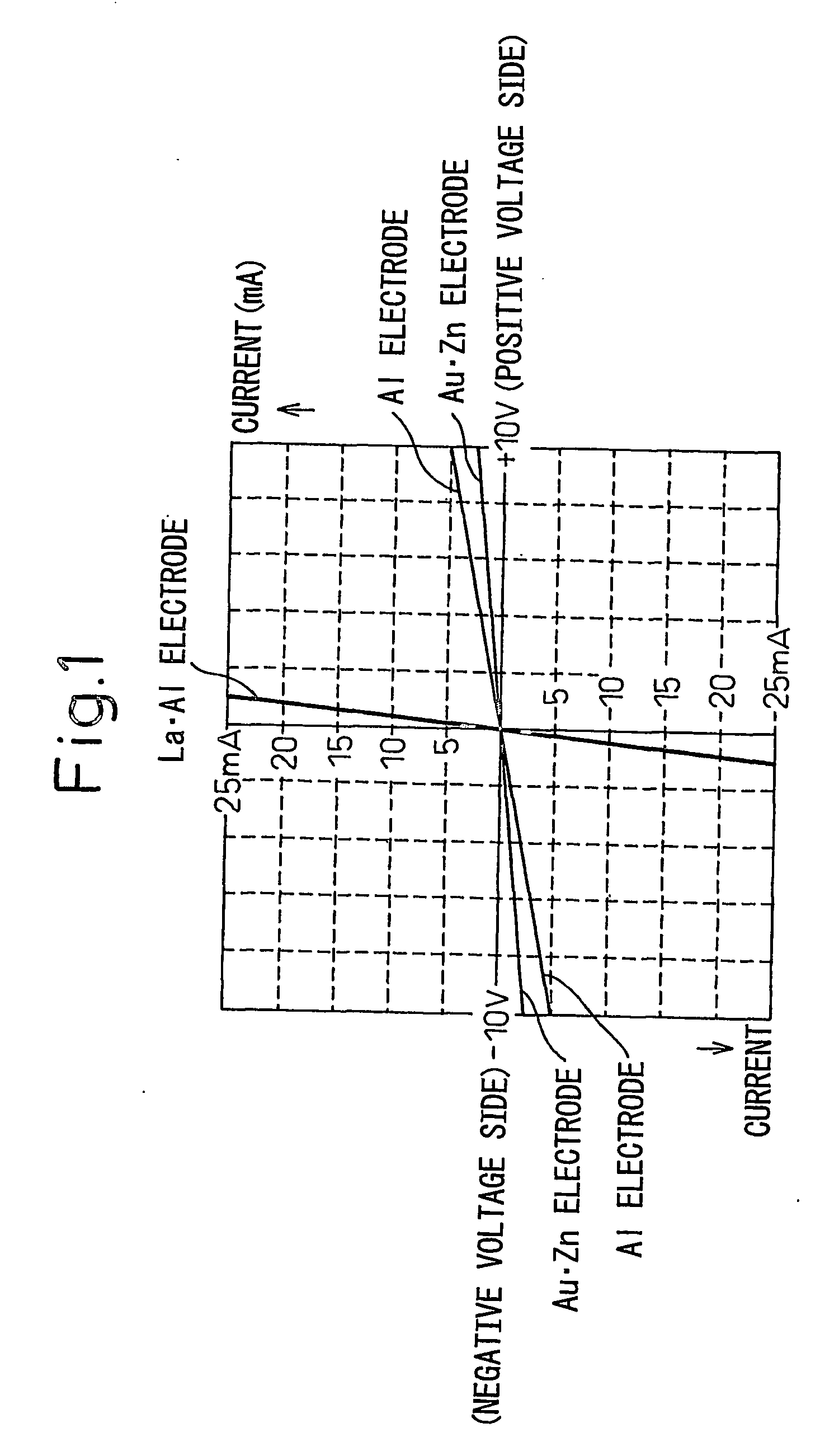
[0054] The present invention will be described in detail by taking as an example a compound semiconductor LED fabricated by providing a p-type Ohmic electrode formed of a lanthanum-aluminum alloy (LaAl2) on the surface of a p-type boron phosphide-base semiconductor layer.
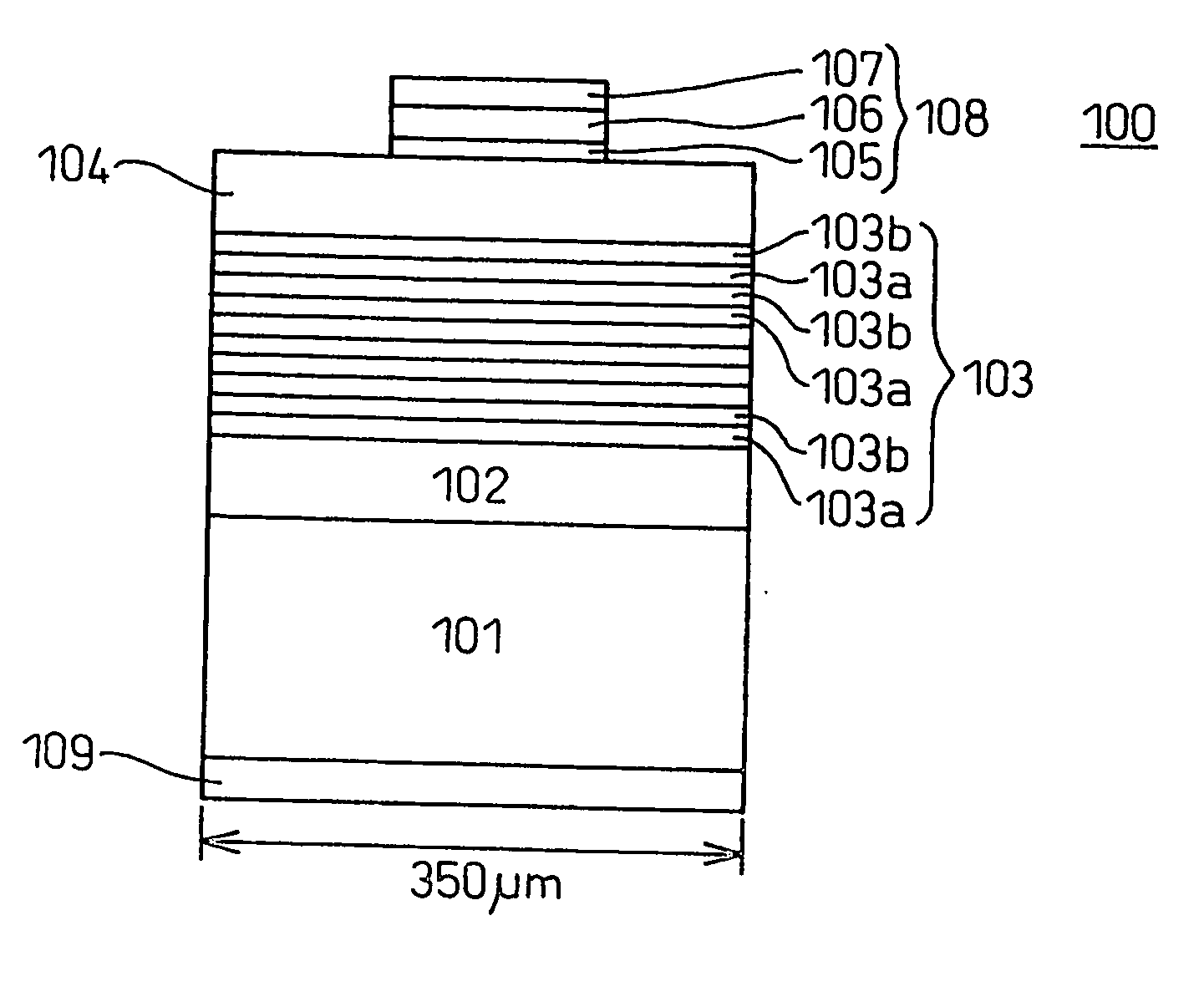
[0055]FIG. 2 schematically shows a cross-section of a stacked structure employed for fabricating an LED 100 having a double-hetero (DH) junction structure. The stacked structure was fabricated by sequentially depositing, on a phosphorus (P)-doped n-type (111)-silicon (Si) single-crystal substrate 101, a lower cladding layer 102 formed of undoped n-type boron phosphide (BP); a light-emitting layer 103 having a multi-layer quantum well structure including five units, each unit consisting of a n-type gallium indium nitride (Ga0.90In0.10N) well layer 103a and a gallium nitride (GaN) barrier layer 103b; and an upper cladding layer 104 formed of undoped p-type boron phosphide.
[0056] The undoped n-type and p-type boron p...
example 2
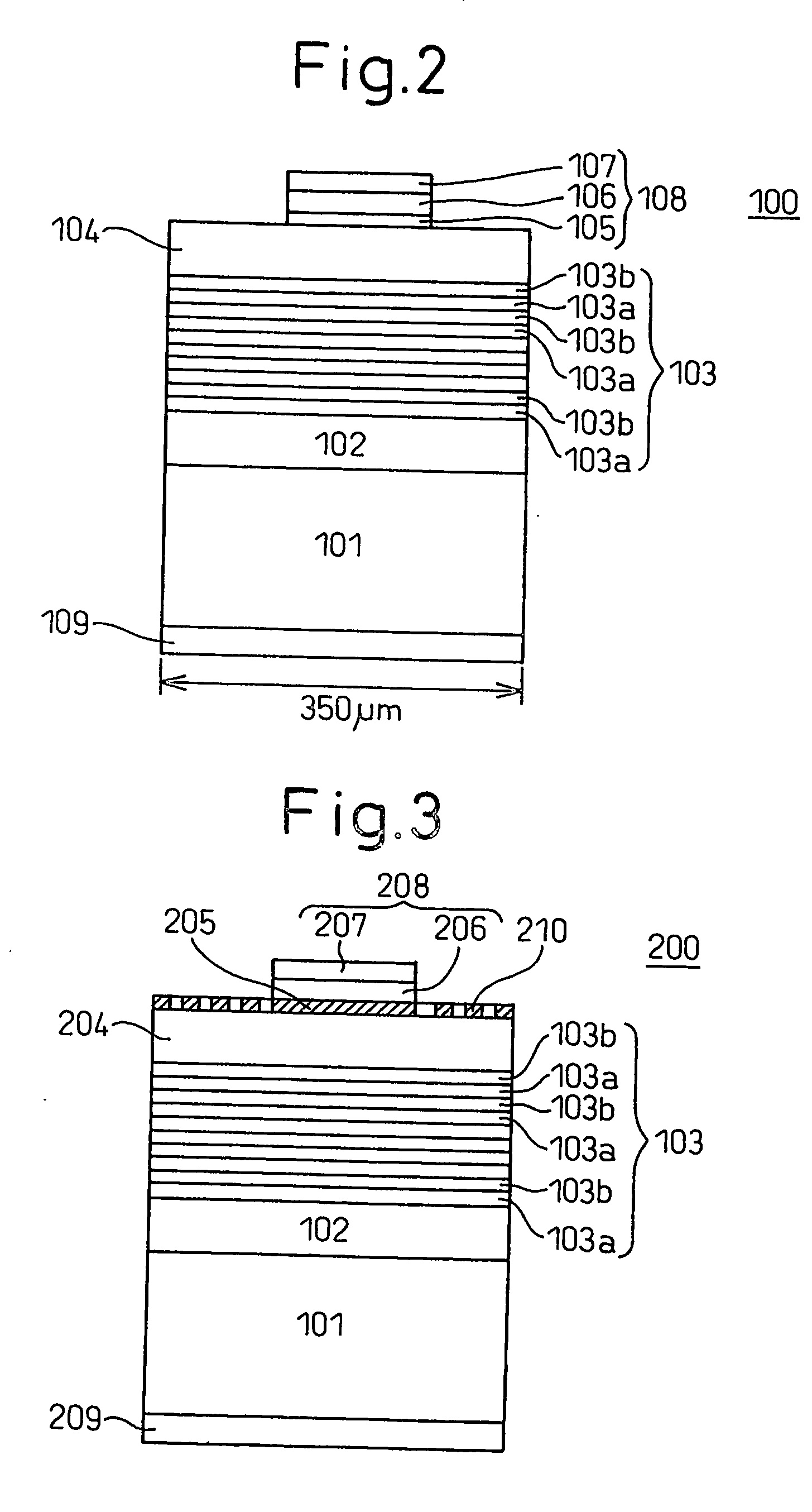
[0062] The present invention will be described in detail by taking as an example a compound semiconductor LED fabricated by providing a p-type Ohmic electrode formed of a lanthanum-silicon alloy on the surface of a p-type boron gallium phosphide mixed crystal layer. The essential structure of the compound semiconductor light-emitting device of Example 2 is the same as that of the LED of Example 1, and the same members are represented by the same reference numerals as employed in Example 1. FIG. 3 is a cross-section of and FIG. 4 is a plan view of the device of Example 2.
[0063] On the light-emitting layer 103 mentioned in the aforementioned Example 1, an undoped p-type boron gallium phosphide mixed crystal (B0.98Ga0.02P) layer 204 was deposited. The B0.98Ga0.02P layer 204 was formed through reduced-pressure MOCVD means at 850° C. using a (C2H5)3B / (CH3)3Ga / PH3 system. The thickness of the layer was controlled to 340 nm. The carrier concentration and the resistivity of the B0.98Ga0.02...
PUM
 Abstract
Description
Claims
Application Information


