
Multiwell sample plate with integrated impedance electrodes and connection scheme

a multi-well sample plate and impedance electrode technology, applied in the field of screening devices, can solve the problems of reducing throughput speed, not allowing, and adding a level of complexity to the high throughput process

Inactive Publication Date: 2006-09-28
MOLECULAR DEVICES +1
View PDF5 Cites 85 Cited by
  • Summary
  • Abstract
  • Description
  • Claims
  • Application Information

AI Technical Summary

Benefits of technology

[0013] Multi-well assay plates typically are made in standard sizes and shapes and having standard arrangements of wells. Some well established arrangements of wells include those found on 96-well plates, 384-well plates and 1536-well plates and 9600-well plates, with the wells configured in two-dimensional arrays. Other formats may include single well plates (preferably having a plurality of assay domains), 2 well plates, 6 well plates, 24 well plates, and 6144 well

Problems solved by technology

Because the insertion of an electrode structure into each plate well adds an additional level of complexity to the high throughput process and reduces throughput speed, integrated electrodes were needed.
Protruding electrodes measure the bulk of the fluid in the microwell and do not allow for the measurement of a deposition of a layer of cells upon the electrodes.
Because redox reactions are traditionally conducted using direct voltage and the current flow associated with redox reactions would upset the electrochemical equilibrium of any cellular system, the integrated redox electrode structure cannot be used for systems that seek to monitor real-time cellular activation.
Along with the advantages of electrical testing in multiwell plates, one of the challenges that emerges is the large number of electrical contacts required as the number of wells increases.
Though in some applications the number of required electrical contacts may be reduced by connecting one or more conductors together (for instance, electrodes sharing a common ground line), there are applications in which this is not desired due to potential interferences between wells sharing connected conductors and the reduction in capability to simultaneously measure multiple wells.
For the larger number of required electrical connections, edge connections become inconvenient.

Method used


Image

  • Multiwell sample plate with integrated impedance electrodes and connection scheme
  • Multiwell sample plate with integrated impedance electrodes and connection scheme
  • Multiwell sample plate with integrated impedance electrodes and connection scheme

Examples


example 1

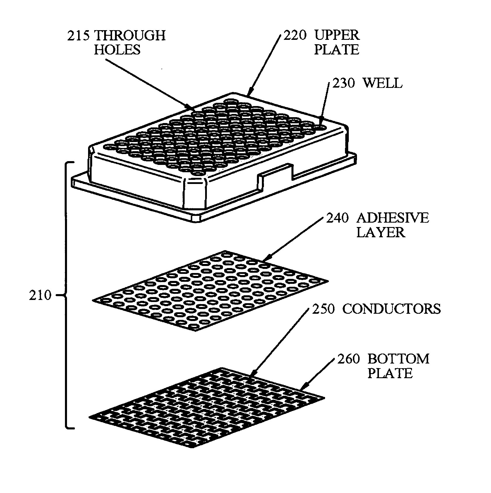
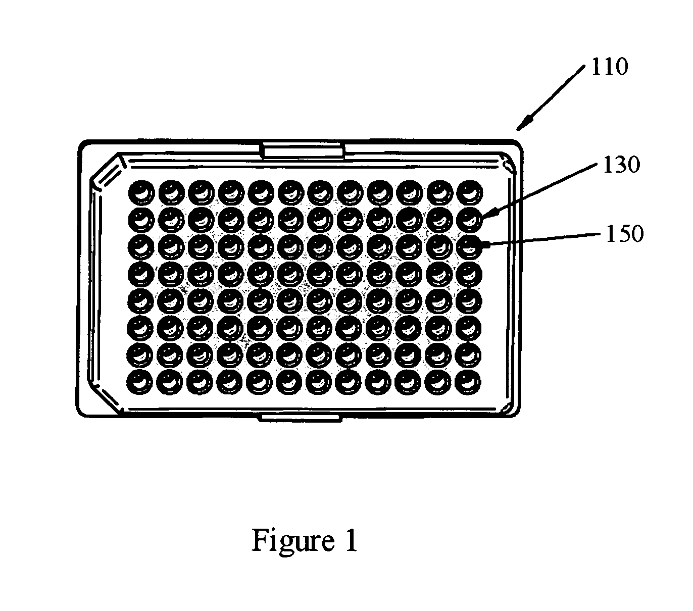
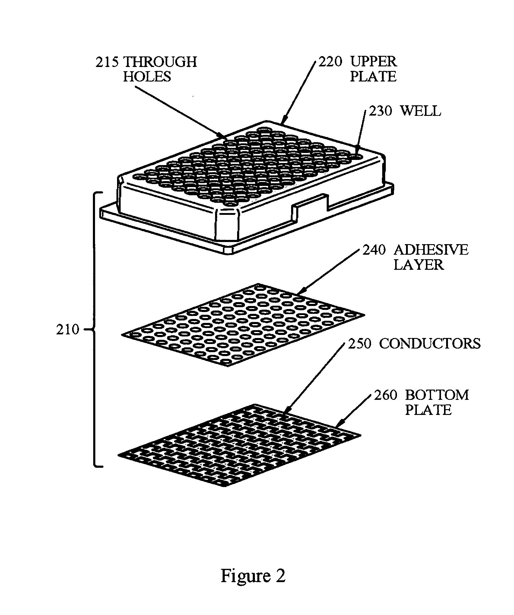
[0060] A bottom plate was fabricated from a 1 mm thick 122 mm×79 mm Borofloat™ glass substrate. Holes in the glass (0.030″) were drilled using an ultrasonic process. 1.6 microns of gold was sputtered onto both the top and bottom surfaces of the glass. At the same time, sputtered gold coated the inside surface of the drilled holes, forming an electrical via between to top and bottom surfaces of the glass. Photolithographic exposure and chemical etching techniques were then used to pattern the impedance measuring electrodes on the top surface of the bottom plate and to form the electrical contact pads on the bottom surface of the bottom plate. The electrodes were a pair of interdigitated finger combs with finger sizes of 30 microns in width and 2.5 mm in length. Gaps between the fingers on opposing combs were 30 microns.

[0061] The bottom plate was bonded using UV curable epoxy to a machined polystyrene upper plate containing 96 through holes in an 8×12 array. The 96 holes, each 6 mm ...

example 2

[0064] A bottom plate was fabricated from a 1 mm thick 122 mm×79 mm polystyrene sheet substrate. Holes in the polystyrene (0.030″) were drilled. 0.5 microns of gold was sputtered onto the top surface of the polystyrene through a thin metal mask or stencil in order to create the electrode pattern. The electrodes were a pair of interdigitated finger combs with finger sizes of 200 microns in width and 1.5 mm in length. Gaps between the fingers on opposing combs were 200 microns. At the same time as the electrodes were created, sputtered gold coated the inside surface of the drilled holes. Subsequently, 0.5 microns of gold was sputtered onto the bottom surface of the polystyrene through a thin metal mask or stencil in order to create the electrical contact pad pattern. At the same time, sputtered gold again coated the inside surface of the drilled holes, forming an electrical via between to top and bottom surfaces of the polystyrene. After fabrication of the gold features on the polysty...

example 3

[0069] Bottom plates were fabricated from a 0.005″ thick polyester sheet substrate. Holes in the polystyrene (0.15 mm) were laser drilled in a pattern to match with the electrical vias to be created in a later step in the bottom plate. Conductive silver ink was used in a screen printing process to create the electrical contact pads on the bottom surface of the bottom plate material and to fill into the drilled via holes. Subsequently, a second printing pass with silver ink was used to print features on the top surface of the bottom plate, leading from the drilled vias towards a location near where the center of the microplate wells will be created when the bottom plate and upper plate are bonded. Subsequently, fingers of gold ink were printed creating an interdigitated finger pattern between the two silver leads. Each gold finger overlapped on one end with one of the silver leads. In the last printing step, a dielectric ink was printed, covering the entire surface top surface of the...


PUM


Abstract

As disclosed within, the present device is directed to a multi-well sample module having integrated impedance measuring electrodes (which allow for the generation of an electric field within each well and the measuring of the change in impedance of each of the well's contents) and an electrical connection scheme allowing simultaneous measurement of each well's change in impedance.

Description

FIELD OF THE INVENTION [0001] The present device relates to screening devices for label-free, real-time detection of cellular activation. [0002] With the advent of combinatorial library methods for generating large libraries of compounds as well as improvements in miniaturization and automation of chemical and biological experiments, there has been a growing interest in methods for screening such libraries for binding with molecular targets, either in the presence or absence of the biological (cellular) environment. HTS Methods [0003] The most widely used screening method involves competitive or non-competitive binding of library compounds to a selected target protein, such as an antibody or receptor utilizing labeled agonists. This method is often conducted in a high throughput screening apparatus consisting of a multi-well device defining a plurality of discrete micro-wells on a substrate surface and measuring structures in each well. A variety of techniques have been developed f...

Claims


Application Information

Patent Timeline
IPC IPC(8): B01L3/00
CPCB01L3/5085B01L2200/0647B01L2300/021B01L2300/0645B01L2300/1827G01N33/48728B01L3/00G01N27/02G01N27/07
Inventor FULLER, CHRIS K.SUGARMAN, JEFFREY H.
Owner MOLECULAR DEVICES
Features
  • Generate Ideas
  • Intellectual Property
  • Life Sciences
  • Materials
  • Tech Scout
  • Unparalleled Data Quality
  • Higher Quality Content
  • 60% Fewer Hallucinations
Learn More