Light-emitting device and method for manufacturing light-emitting device

Inactive Publication Date: 2006-10-05
SHIN-ETSU HANDOTAI CO LTD
View PDF8 Cites 20 Cited by
  • Summary
  • Abstract
  • Description
  • Claims
  • Application Information

AI Technical Summary

Benefits of technology

[0014] Various structural sophistication can be made on the active layer and the p-type cladding layer, in order to obtain intrinsic or p-type semiconductor with good quality. For example, it is allowable to adopt a configuration in which a p-type oxide layer, which is different from MgaZn1-aO-type oxide and shows p-type conductivity, is inserted in a MgZnO layer composing the active layer or the cladding layer. In this configuration, the p-type oxide layer locally presents in the MgZnO layer can participate in functions of absorbing and compensating electrons, so that it is no more necessary to add a large amount of p-type dopant, it is made possible to obtain a p-type or i-type MgaZn1-aO-type oxide with good quality, and it is consequently made possible to realize a ultraviolet or blue light emitting device of high emission luminance. Although there is no specific limitation on the number of layers of the p-type oxide layer, it is of course preferable that the electron compensation effect can be exhibited uniformly over the entire MgZnO layer in expectation of a high emission luminance. For this purpose, it is preferable to form a plurality of p-type oxide layers in a distributed manner, for example in a periodic manner, in the thickness-wise direction of the MgZnO layer. As the p-type oxide layer, a layer mainly composed of any of CuO, NiO and LiO can be used. For the case where CuO is adopted, a part of Cu may be substituted by a Group III element such as Ga, or by a Group II element such as Sr.
[0015] In the p-type cladding layer, it is allowable to form a high concentration doped layer having a p-type dopant concentration larger than an average concentration of the p-type cladding layer, as having a zonal width of not larger than a single-molecular layer of the p-type cladding layer (so-called δ doped layer). By forming the high concentration doped layer containing a p-type dopant, in the p-type cladding layer, so as to attain a zonal width of not larger than a single-molecular layer of the p-type cladding layer, the p-type dopant are, as it were, localized in the thickness-wise direction. Because the high-concentration doped layer, which is the localized layer of the p-type dopant, can function as absorbing and compensating electrons, it is no more necessary to add a large amount of p-type dopant, and thereby the p-type cladding layer having good quality can be obtained. The-high-concentration doped layer is also advantageous in that it is less likely to produce mismatched heterogeneous interface and dislocation, which are causative of scattering of carriers, because the layer is formed as having a zonal width of not larger than a single-molecular layer of the p-type cladding layer, in place of forming a coarse heterogeneous crystal grains as an aggregates of the p-type dopant.
[0016] In the light emitting device of this invention, MgaZn1-aO-type oxide can be formed by vapor phase growth process. Recognizing now possibility of adop

Problems solved by technology

The MgaZn1-aO-type oxide, however, needs a highly sophisticated technology to be obtained as a p-type semiconductor, raising a considerable difficulty in obtaining in particular a high conductivity p-type semiconductor.
The electron density ascribable to the oxygen deficiency may however reach as maximum as an order of 1019 cm−3 or above, so that any efforts of completely compensating such a large amount of electrons by uniform doping of a p-type dopant

Method used


Image

  • Light-emitting device and method for manufacturing light-emitting device
  • Light-emitting device and method for manufacturing light-emitting device
  • Light-emitting device and method for manufacturing light-emitting device

Examples


Example

[0028] The following paragraphs will describe best modes for carrying out this invention, referring to the attached drawings.

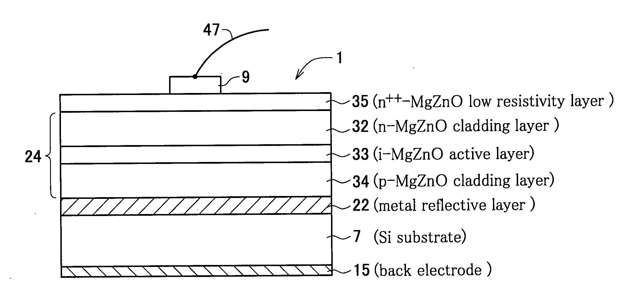
[0029]FIG. 1 schematically shows, in a form of stacked structure, an essential portion of a light emitting device 1 as one embodiment of this invention, having a light emitting layer section 24 in which an n-type cladding layer 32, an active layer 33 and a p-type cladding layer 34 are stacked in this order. Each of the layers 32 to 34 is formed as a MgaZn1-aO-type oxide layer (0≦a≦1: also referred to as MgZnO hereinafter: it is to be noted that a notation MgZnO includes concepts of both of simple oxides MgO and ZnO, as is obvious from the variable range for alloy composition “a”).

[0030] The light emitting device 1 uses a face on the n-type cladding layer 32 side a light extraction surface, and has, as being formed on the main surface on the light extraction surface side of the n-type cladding layer 32, an n-type low resistivity layer 35 composed of a MgaZn1-...


PUM


Abstract

A light emitting device 1 has formed therein a light emitting layer section 24 based on a double heterostructure in which a p-type cladding layer 34, an active layer 33 and an n-type cladding layer 32, individually composed of a MgaZn1-aO (0≦a≦1) type oxide, are stacked in this order, and uses a face on the n-type cladding layer side as a light extraction surface. The device also has, as being provided on the main surface on the light extraction surface side of the n-type cladding layer 32, an n-type low resistivity layer 35 composed of a MgaZn1-aO type oxide, and having a content of an n-type dopant larger than that in the n-type cladding layer 32. There is thus provided a light emitting device of MgaZn1-aO-type oxide base, excellent in the light extraction efficiency, having the light emitting layer section composed of a MgaZn1-aO-type oxide, and a high conductivity MgZnO-base compound semiconductor layer disposed on the light extraction surface side.

Description

FIELD OF THE INVENTION [0001] This invention relates to a light emitting device using semiconductor, in particular to a light emitting device suitable for emission of blue light or ultraviolet radiation, and a method of fabricating the same. BACKGROUND ART [0002] High luminance light emitting devices capable of short-wave emission in the blue light region have long been expected, and this sort of light emitting devices have recently realized by using AlGaInN-base materials. Rapid progress has also been made in application to full-color light emitting devices and display devices, based on combination with red and green high luminance light emitting devices. AlGaInN-base materials cannot, however, avoid increase in the cost because they are mainly composed of Ga and In, which are relatively rare-existing metals. Another big problem is that the material need growth temperature of as high as 700 to 1,000° C., causing a considerably large energy consumption for the manufacture. This is u...

Claims


Application Information

Patent Timeline
IPC IPC(8): H01L33/00H01L21/365H01L33/28H01L33/40H01S5/32
CPCH01L33/28
Inventor ISHIKAZI, JUN-YA
Owner SHIN-ETSU HANDOTAI CO LTD
Why Eureka
Try Eureka