Semiconductor device and its manufacture method

a technology of semiconductors and manufacturing methods, applied in the direction of semiconductor devices, basic electric elements, electrical equipment, etc., can solve the problems that the desired results cannot be obtained in some cases, and achieve the effect of good high-voltage transistor characteristics without adversely affecting the characteristics of low-voltage transistors

Inactive Publication Date: 2006-10-05
FUJITSU LTD
View PDF6 Cites 43 Cited by
  • Summary
  • Abstract
  • Description
  • Claims
  • Application Information

AI Technical Summary

Benefits of technology

[0022] Thermal oxidation for STI surrounding the high voltage transistor area is performed separately from thermal oxidation for STI surrounding the low voltage transistor area. It is therefore possible to retain good high voltage transistor characteristics without adversely affecting low voltage transistors characteristics.

Problems solved by technology

Reliability of an insulated gate structure is an important issue of high breakdown voltage transistors.
If a plurality type of transistors are to be integrated, the manufacture processes are influenced each other so that desired results cannot be obtained in some cases.

Method used


Image

  • Semiconductor device and its manufacture method
  • Semiconductor device and its manufacture method
  • Semiconductor device and its manufacture method

Examples


first embodiment

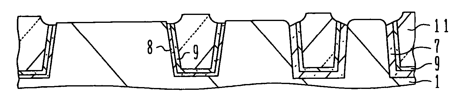
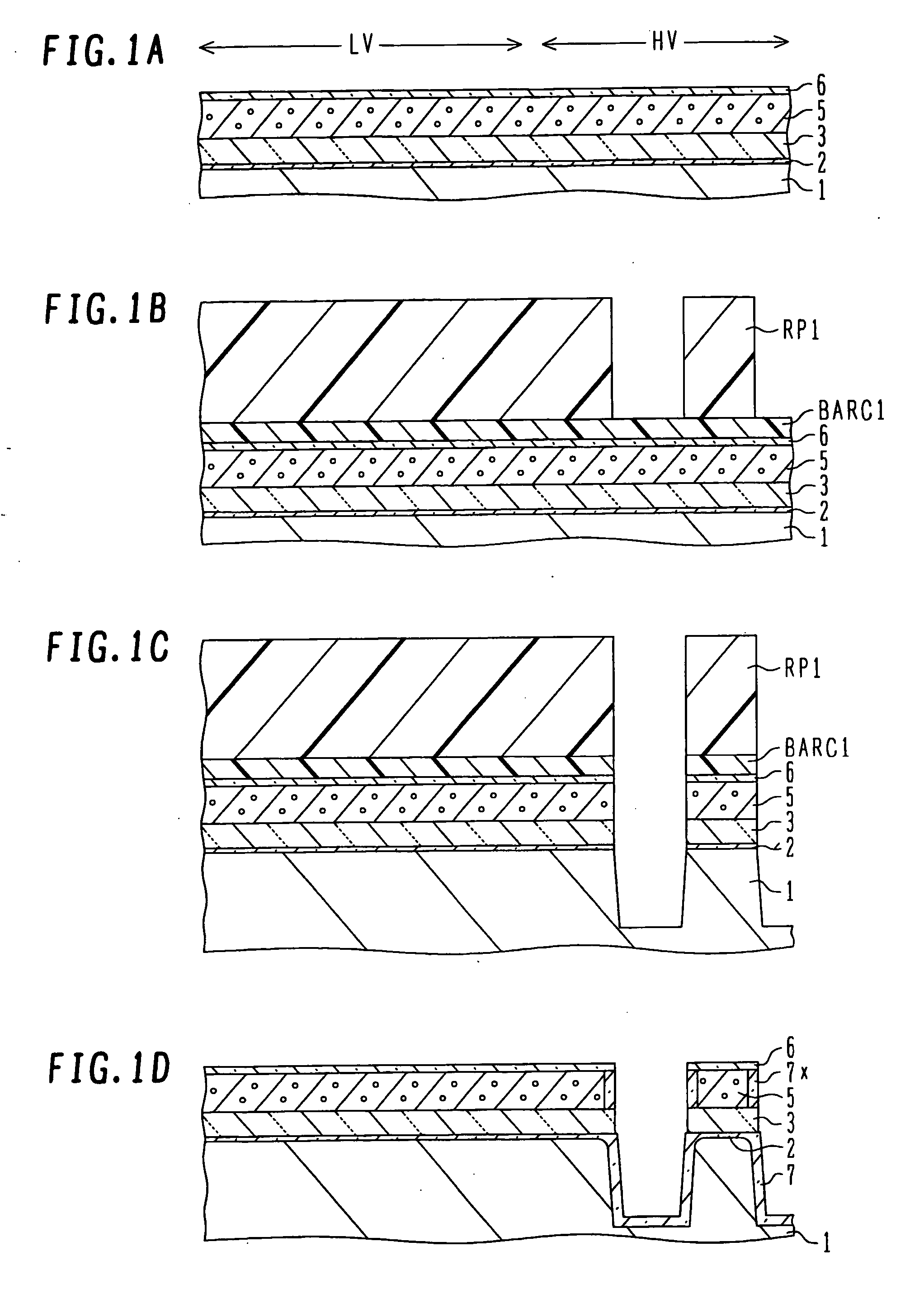
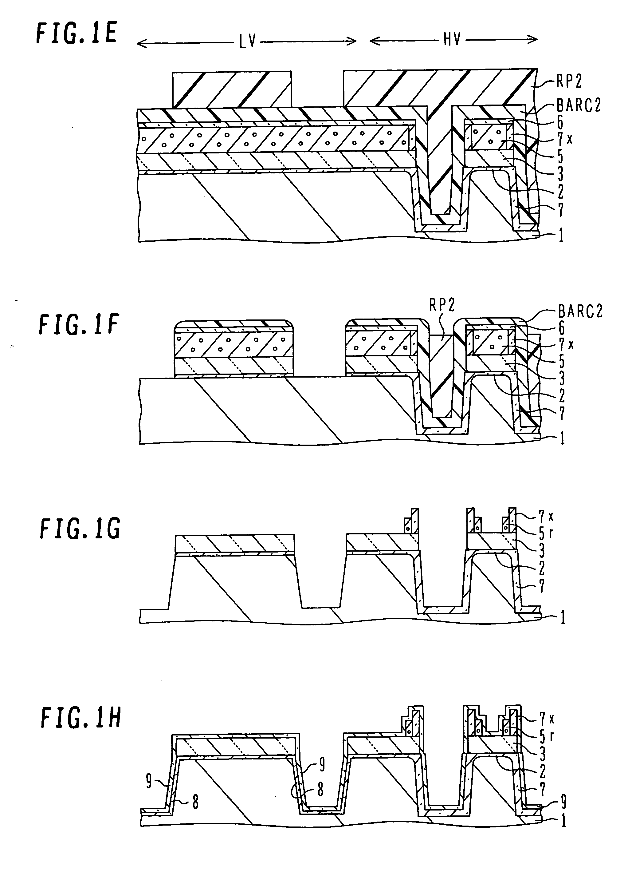
[0030]FIG. 1A to 1L are cross sectional views of a semiconductor substrate illustrating a semiconductor device manufacture method and its modification of the present invention.

[0031] As shown in FIG. 1A, a semiconductor substrate 1 made of, e.g., p-type silicon, has a low voltage area LV shown in left and a high voltage area HV shown in right. A thermal oxide film 2 having a thickness of 10 nm is grown on the surface of a semiconductor substrate, for example, by thermal oxidation, and a silicon nitride film 3 having a thickness of 120 nm is grown on the thermal oxide film by low pressure (LP) chemical vapor deposition (CVD). A polysilicon film 5 having a thickness of 150 nm is grown on the silicon nitride film 3 by CVD and a silicon nitride film 6 having a thickness of 7 nm is grown on the polysilicon film by CVD. The silicon nitride film functions as an anti-oxidation film for the polysilicon film. These films are used as a hard mask and have a stopper function for chemical mechan...

second embodiment

[0046]FIGS. 2A to 2K are cross sectional views of a semiconductor substrate illustrating the second embodiment and its modification.

[0047] As shown in FIG. 2A, the surface of a silicon substrate 1 is thermally oxidized to form a thermal oxide film 2 having a thickness of about 10 nm, and a silicon nitride film 3 having a thickness of about 120 nm is deposited on the thermal oxide film by LPCVD.

[0048] As shown in FIG. 2B, a BARC 3 film having a thickness of about 80 nm and a KrF resist film having a thickness of about 500 nm are coated on the silicon nitride film 3, and the resist film is exposed with KrF excimer laser and developed to form a resist pattern RP4. By using the resist pattern RP4 as an etching mask, similar to the first embodiment, the BARC 3 film, silicon nitride film 3 and silicon oxide film 2 are etched and the silicon substrate 1 is etched by a depth of about 300 nm. The resist pattern RP4 is thereafter removed.

[0049] As shown in FIG. 2C, the silicon oxide film 2 ...

third embodiment

[0078] Two photolithography processes complicate the manufacture processes. It is possible to form an isolation trench both in the low voltage transistor area and high voltage transistor area at the same time. FIGS. 3A to 3G are cross sectional views illustrating a semiconductor device manufacture method according to the

[0079] As shown in FIG. 3A, the surface of a silicon substrate 1 is thermally oxidized to form a thermal oxide film 2 having a thickness of 10 nm. A silicon nitride film 3 is grown on the thermal oxide film to a thickness of 120 nm by LPCVD. A polysilicon layer 5 is grown on the silicon nitride film to a thickness of 150 nm. A BARC film is coated on the polysilicon layer 5 to a thickness of about 80 nm, and an ArF resist film ArR is coated on the BARC film. Since the minimum pattern width in the low voltage transistor area is about 120 nm, a thickness of the resist film ArR is set to about 300 nm. The resist film ArR is exposed with ArF excimer laser and developed to...


PUM


Abstract

A semiconductor device includes: a semiconductor substrate; and STIs formed in the semiconductor substrate and defining a high voltage transistor area and a low voltage transistor area, the STIs including: a first STI with a first liner including a thermal oxide film and not including a nitride film and surrounding at least a portion of the high voltage transistor area; and a second STI with a second liner of a lamination of a thermal oxide film and a nitride film and surrounding the low voltage transistor area.

Description

CROSS REFERENCE TO RELATED APPLICATION [0001] This application is based on and claims priority of Japanese Patent Application No. 2005-102693 filed on Mar. 31, 2005, the entire contents of which are incorporated herein by reference. BACKGROUND OF THE INVENTION [0002] A) Field of the Invention [0003] The present invention relates to a semiconductor device and its manufacture method, and more particularly to a composite semiconductor device integrating low voltage, high speed operation micro semiconductor elements and high breakdown voltage semiconductor elements and to its manufacture method. [0004] B) Description of the Related Art [0005] In the broadband age, merger and adaptation to multimedia of consumer-related equipments and IT-related equipments are accelerated with the developments of digitalization. With such rapid change, it is requested to expand the functions of base systems such as servers and communication systems as well as various portable terminal apparatuses and hom...

Claims


Application Information

Patent Timeline
Patent Type & Authority Applications(United States)
IPC IPC(8): H01L29/76
CPCH01L21/76227H01L21/76229H01L21/823878H01L27/11546H01L27/105H01L27/11519H01L27/11526H01L27/0207H10B41/10H10B41/40H10B41/49
Inventor ANEZAKI, TORUOGURA, JUSUKEEMA, TAIJI
Owner FUJITSU LTD
Why Eureka
Try Eureka