Semiconductor device

a technology of semiconductors and devices, applied in the field of semiconductor devices, can solve the problems of reducing the performance of pae under the low distortion condition, reducing the efficiency of the device, and difficult to obtain the low distortion, etc., and achieve the effect of facilitating the control of the zn diffusion

Inactive Publication Date: 2006-10-05
SONY CORP
View PDF4 Cites 24 Cited by
  • Summary
  • Abstract
  • Description
  • Claims
  • Application Information

AI Technical Summary

Benefits of technology

[0025] For a case where the p-type conductive region in the first barrier layer is formed by diffusing Zn, the invention (4) makes it possi...

Problems solved by technology

Reduction in the distortion is also a critical issue because recent mobile terminals based on use of wireless communication system such as CDMA (Code Division Multiple Access) and WCDMA (Wideband CDMA) are in need of more strict specifications with respect to distortion of the power amplifiers.
Improvement of power amplifier characteristics in the HBT application needs an increased current density, but this may result in a problem due to heat generation, or this may need an advanced design for heat dissipation for ensuring the reliability.
The enhancement-mode HFET realized in a form of conventional Schottky-junction-gate-type HFET having a recessed gate structure, however, raises a first prob...

Method used


Image

  • Semiconductor device
  • Semiconductor device
  • Semiconductor device

Examples


second embodiment

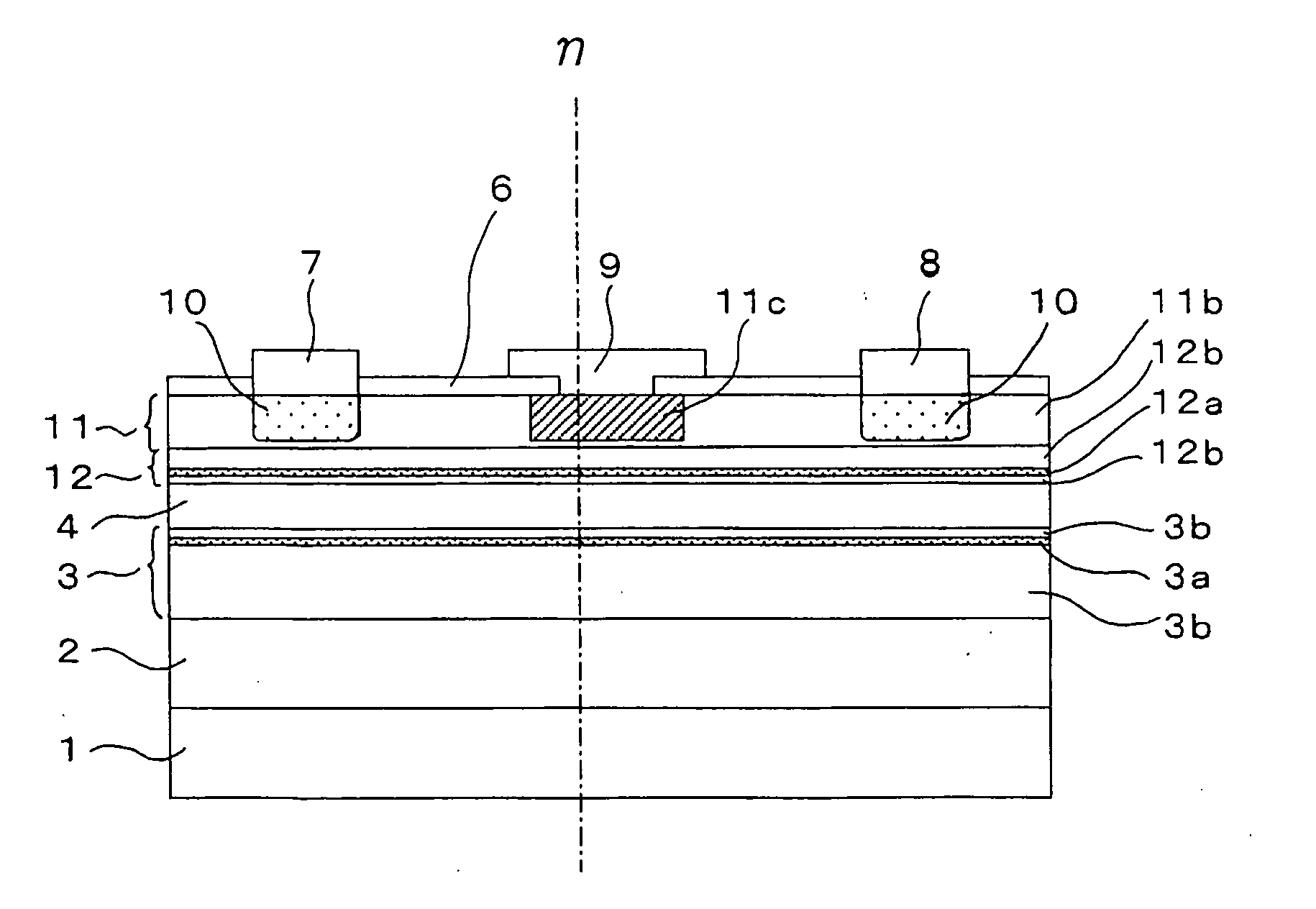
[0051] The next paragraphs will describe the second embodiment of the semiconductor device of the present invention referring to FIG. 3. In comparison with the first embodiment, this embodiment further comprises a fourth barrier layer 14 not intentionally doped with any impurities, between the third barrier layer 13 and the channel layer 4.

[0052] The third barrier layer 13 uses a material satisfying the relation (1) with the first barrier layer 11, similarly to the third barrier layer 12 in the first embodiment, and comprises an n-type impurity heavily-doped region 13a where n-type impurity such as Si is heavily doped, and low-impurity-concentration regions 13b not intentionally doped with any impurities.

[0053] The fourth barrier layer 14 uses a material capable of forming a desirable interface with the channel layer 4, which is typically AlGaAs having an Al composition ratio of, for example, 20% or around or less, or GaAs, not intentionally doped with any impurities. In this case...

third embodiment

[0055] The following paragraphs will describe the third embodiment of the semiconductor device of the present invention referring to FIG. 4. In comparison with the first embodiment, this embodiment does not have a region heavily doped with an n-type impurity in a third barrier layer 15, and further comprises, as being disposed between the third barrier layer 15 and the channel layer 4 a fourth barrier layer 16 having an n-type impurity heavily-doped region 16a.

[0056] The third barrier layer 15 again uses a material satisfying the relation (1) with the first barrier layer 11, similarly to the third barrier layer 12 in the first embodiment, but is not intentionally doped with an n-type impurity.

[0057] On the other hand, the fourth barrier layer 16 uses a material capable of forming a desirable interface with the channel layer 4 similarly to the second embodiment, such as AlGaAs having an Al composition ratio of approximately 20% or less, or GaAs for example, and typically comprises ...

fourth embodiment

[0059] The first embodiment may sometimes raise a problem in ohmic contact resistance between the first barrier layer 11 and the gate electrode 9. In this case, it is advantageous to dispose, on the gate electrode side as shown in FIG. 5, a fifth barrier layer 18 composed of a semiconductor which has a sum of the electron affinity and the band gap smaller than that of the first barrier layer 17.

[0060] The following paragraphs will describe the semiconductor device of the fourth embodiment of the present invention. In this embodiment in comparison with the first embodiment, the first barrier layer 11 is altered to a two-layered configuration comprising a first barrier layer 17 and a fifth barrier layer 18, wherein the fifth barrier layer 18, which is composed of a semiconductor having a sum of the electron affinity and the band gap smaller than that of the first barrier layer 17 is disposed between the first barrier layer 17 and the gate electrode 9.

[0061] The fifth barrier layer 1...


PUM


Abstract

There is provided a semiconductor device capable of ensuring a complete enhancement-mode operation and realizing a power transistor excellent in the low-distortion, high-efficiency performance. On a surface of a substrate (1) composed of single crystal GaAs, a second barrier layer (3) composed of AlGaAs, a channel layer (4) composed of InGaAs, a third barrier layer (12) composed of InGaP and a first barrier layer (11) composed of AlGaAs are stacked in this order, while placing in between a buffer layer (2). Relation of χ1−χ3≦0.5*(Eg3-Eg1), where χ1 is electron affinity of the first barrier layer (11), Eg1 is a band gap of the same, χ3 is electron affinity of the third barrier layer (12), and Eg3 is a band gap of the same, is satisfied between the first barrier layer (11) and the third barrier layer (12).

Description

TECHNICAL FIELD [0001] The present invention relates to a semiconductor device applicable to power amplifiers and so forth. BACKGROUND ART [0002] Low-distortion, high-efficiency operation and single positive power supply operation are recent demands for transmission power amplifiers for mobile terminals for mobile communication. The high-efficiency operation herein means an operation with a high power-added efficiency (referred to as PAE, hereinafter) which is defined by a ratio of difference between output power Pout and input power Pin, and supplied DC power Pdc. PAE is an important figure of merit for power amplifiers because a larger value of PAE means a smaller power consumption. Reduction in the distortion is also a critical issue because recent mobile terminals based on use of wireless communication system such as CDMA (Code Division Multiple Access) and WCDMA (Wideband CDMA) are in need of more strict specifications with respect to distortion of the power amplifiers. Distort...

Claims


Application Information

Patent Timeline
IPC IPC(8): H01L31/07H01L29/808H01L21/285H01L21/335H01L21/337H01L21/338H01L29/778H01L29/812
CPCH01L29/7785H01L29/66462H01L21/28587
Inventor HASE, ICHIRO
Owner SONY CORP
Why Eureka
Try Eureka