High performance PFET header in hybrid orientation technology for leakage reduction in digital CMOS VLSI designs

a hybrid orientation and header technology, applied in the field of very large scale integrated (vlsi) circuit design, can solve the problems of limiting factors such as leakage power (both gate and sub-threshold), and the speed of pfet devices and nfet devices, and achieves low standby leakage power and high performan

Inactive Publication Date: 2006-10-12
IBM CORP
View PDF2 Cites 10 Cited by
  • Summary
  • Abstract
  • Description
  • Claims
  • Application Information

AI Technical Summary

Benefits of technology

[0007] An object of this invention is to provide a CMOS VLSI design

Problems solved by technology

Leakage power (both gate and sub-threshold) is predicted to be the limiting factor in the design of future VLSI systems

Method used


Image

  • High performance PFET header in hybrid orientation technology for leakage reduction in digital CMOS VLSI designs
  • High performance PFET header in hybrid orientation technology for leakage reduction in digital CMOS VLSI designs
  • High performance PFET header in hybrid orientation technology for leakage reduction in digital CMOS VLSI designs

Examples


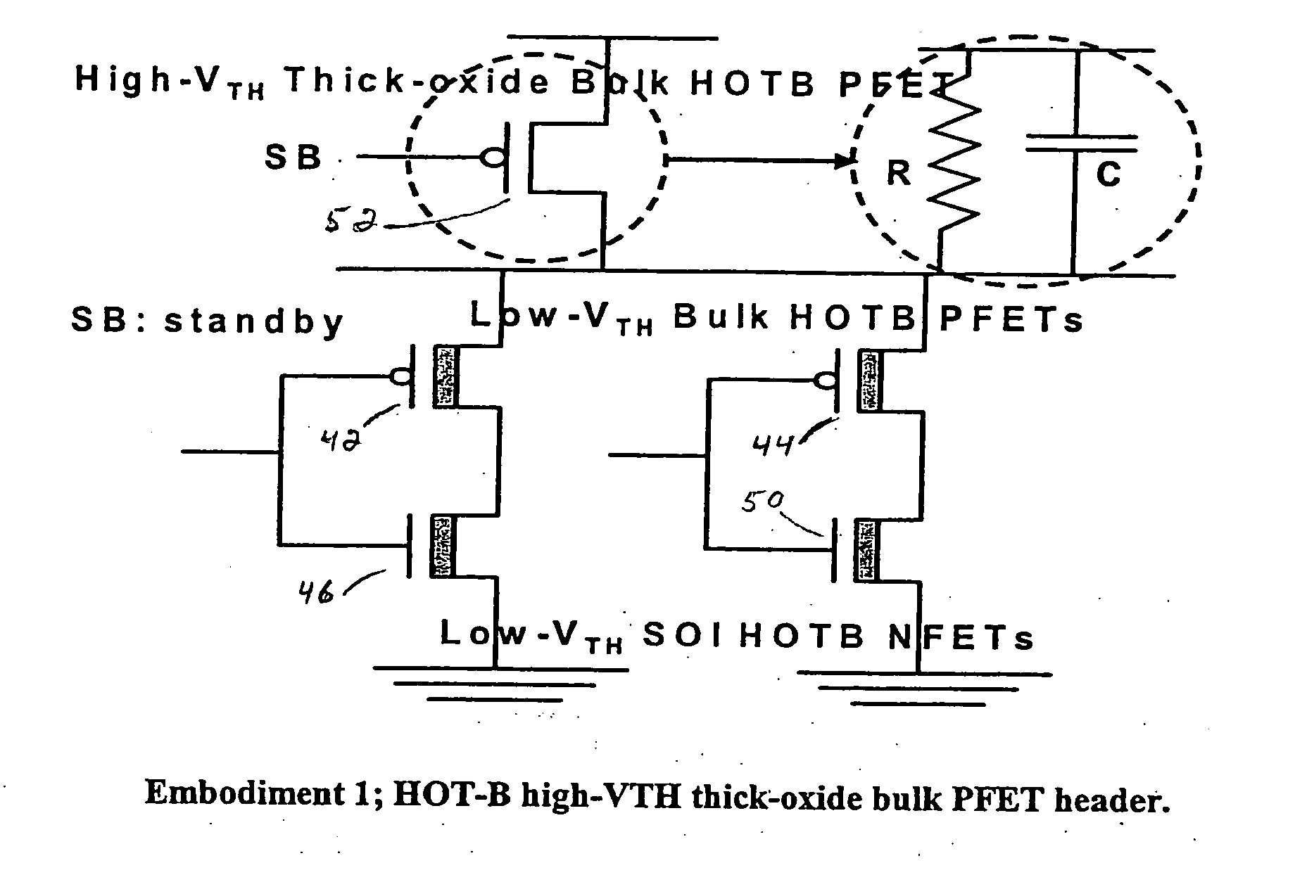
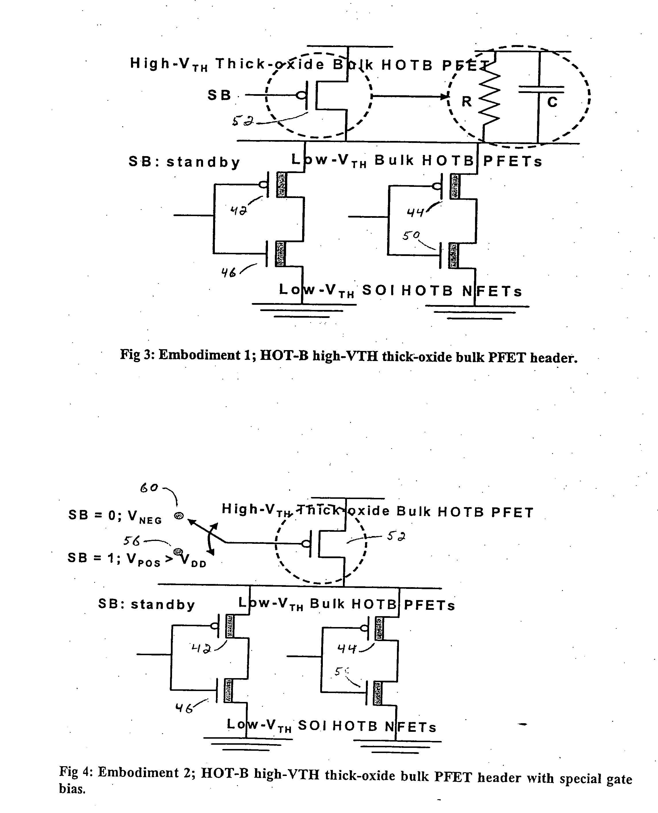
Embodiment Construction

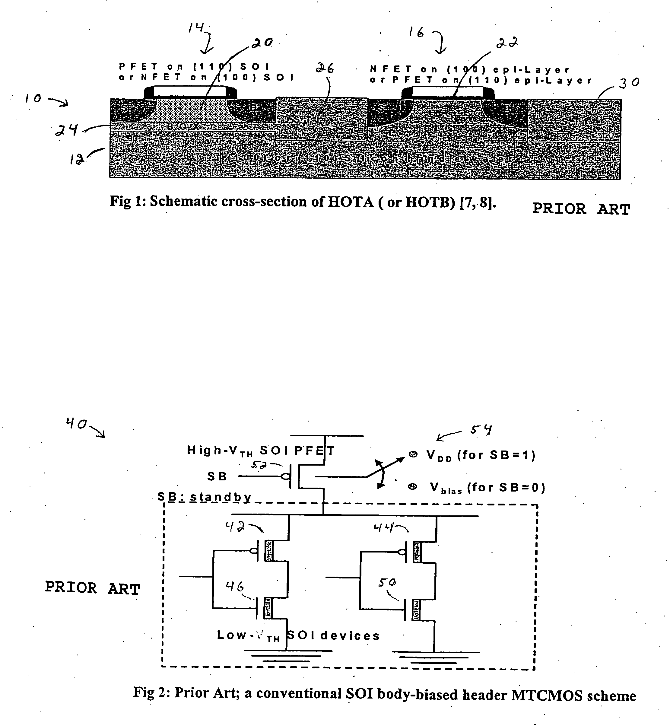
[0024]FIG. 1 is a schematic cross-section illustrating hybrid orientation technology (HOT). More specifically, FIG. 1 shows a portion of a silicon wafer 10 comprising silicon substrate 12 and transistors 14 and 16. Each transistor includes source (S), drain (D) and gate (G) regions, with the source and drain regions separated by a channel region. The channel region of transistor 14 is referenced at 20, and the channel region of transistor 16 is referenced at 22. Beneath transistor 14 is a buried oxide (BOX) region 24, which separates the transistor from the silicon substrate 12. The channel region 22 between the source and drain of transistor 16 is not separated from the silicon substrate and instead is a direct extension of that substrate. A shallow-trench-isolation (STI) region 26 separates transistor 14 from transistor 16, and another STI region 30 is shown in FIG. 1, to the right of transistor 16.

[0025] One of the transistors 14 and 16 is a PFET and the other of these transisto...


PUM


Abstract

Discloses are CMOS circuit designs that combine MTCMOS and hybrid orientation technology to achieve the dual objectives of high performance and low standby leakage power. The invention utilizes novel combinations of a thick-oxide high-VTH PFET header with various gate- and body-biased schemes in HOT technology to significantly reduce the performance penalty associated with conventional PFET headers. A first embodiment of the invention provides a HOT-B high-VTH thick oxide bulk PFET header scheme. This header scheme can be expanded by application of a positive gate bias VPOS (VPOS>VDD) to the HOT-B PFET header during standby mode and a negative gate bias VNEG (VNEG<GND) in active mode. Another embodiment provides a HOT-A high-VTH thick oxide SOI PFET header scheme. A further embodiment provides a HOT-A body biased high-VTH thick oxide SOI PFET header scheme.

Description

BACKGROUND OF THE INVENTION [0001] 1. Field of the Invention [0002] This invention generally relates to very large scale integrated (VLSI) circuit designs. More specifically, the invention relates to leakage reduction in digital CMOS VLSI designs. [0003] 2. Background Art [0004] Leakage power (both gate and sub-threshold) is predicted to be the limiting factor in the design of future VLSI systems. MTCMOS (or VDD-gating) is a very popular technique for controlling standby leakage. It adds a high-VTH PFET header or a high-VTH NFET footer device in series to a circuit to reduce leakage in standby mode. Various other incarnations of MTCMOS have been proposed. The main consideration in the implementation of the MTCMOS scheme is the trade-off between standby leakage power and active mode performance. [0005] In general, a PFET device is slower than an NFET device because of the lower mobility of holes compared with electrons. So, a circuit with a high-VTH PFET header is slower than a circu...

Claims


Application Information

Patent Timeline
IPC IPC(8): H01L29/94
CPCH01L21/823857H01L21/823878H03K19/0016H01L27/1203H01L21/84
Inventor CHUANG, CHING-TE KENTDAS, KOUSHIK KUMARLO, SHIH-HSIEN
Owner IBM CORP
Why Eureka
Try Eureka