Static electricity countermeasure component
- Summary
- Abstract
- Description
- Claims
- Application Information
AI Technical Summary
Benefits of technology
Problems solved by technology
Method used
Image
Examples
first embodiment
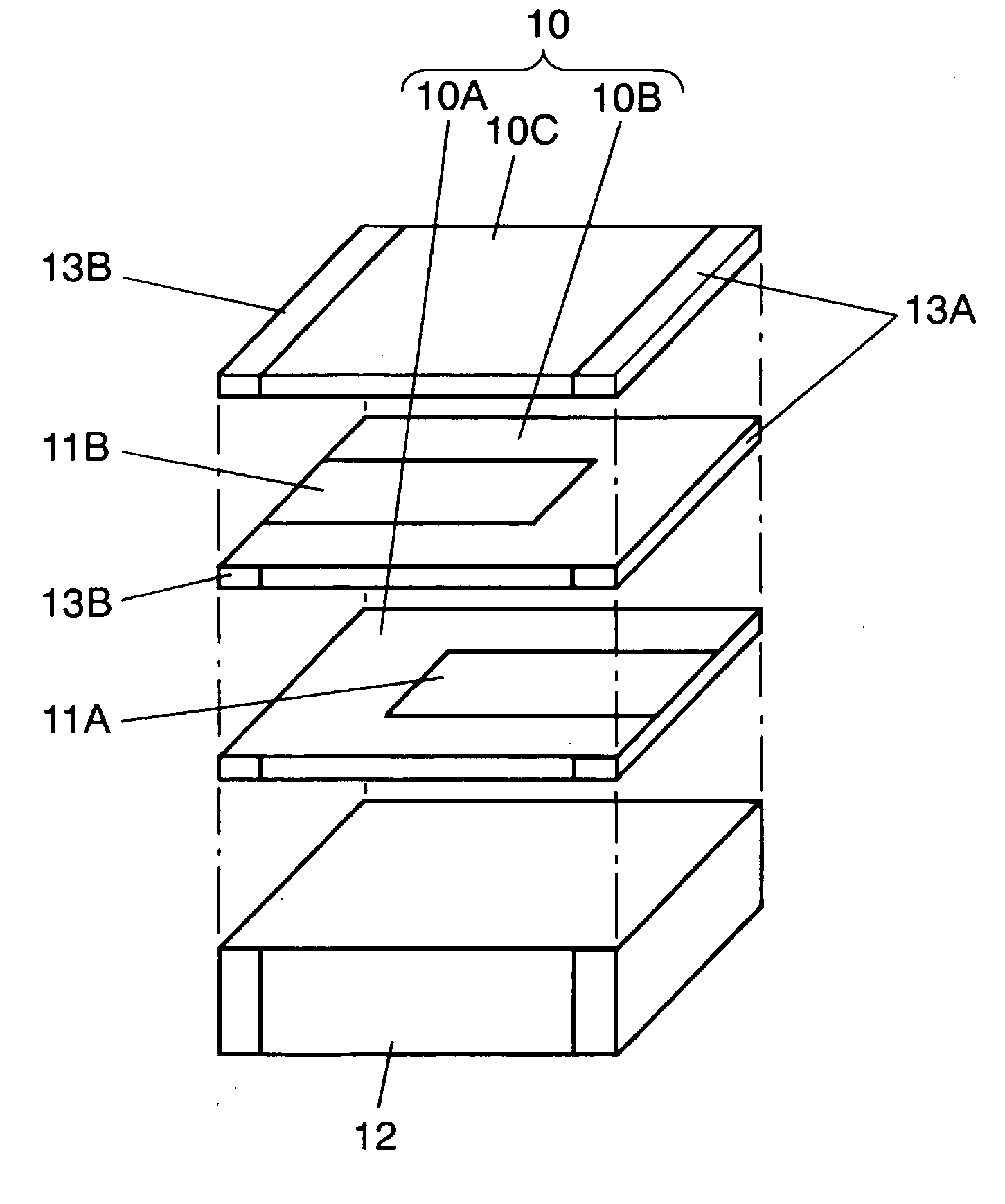
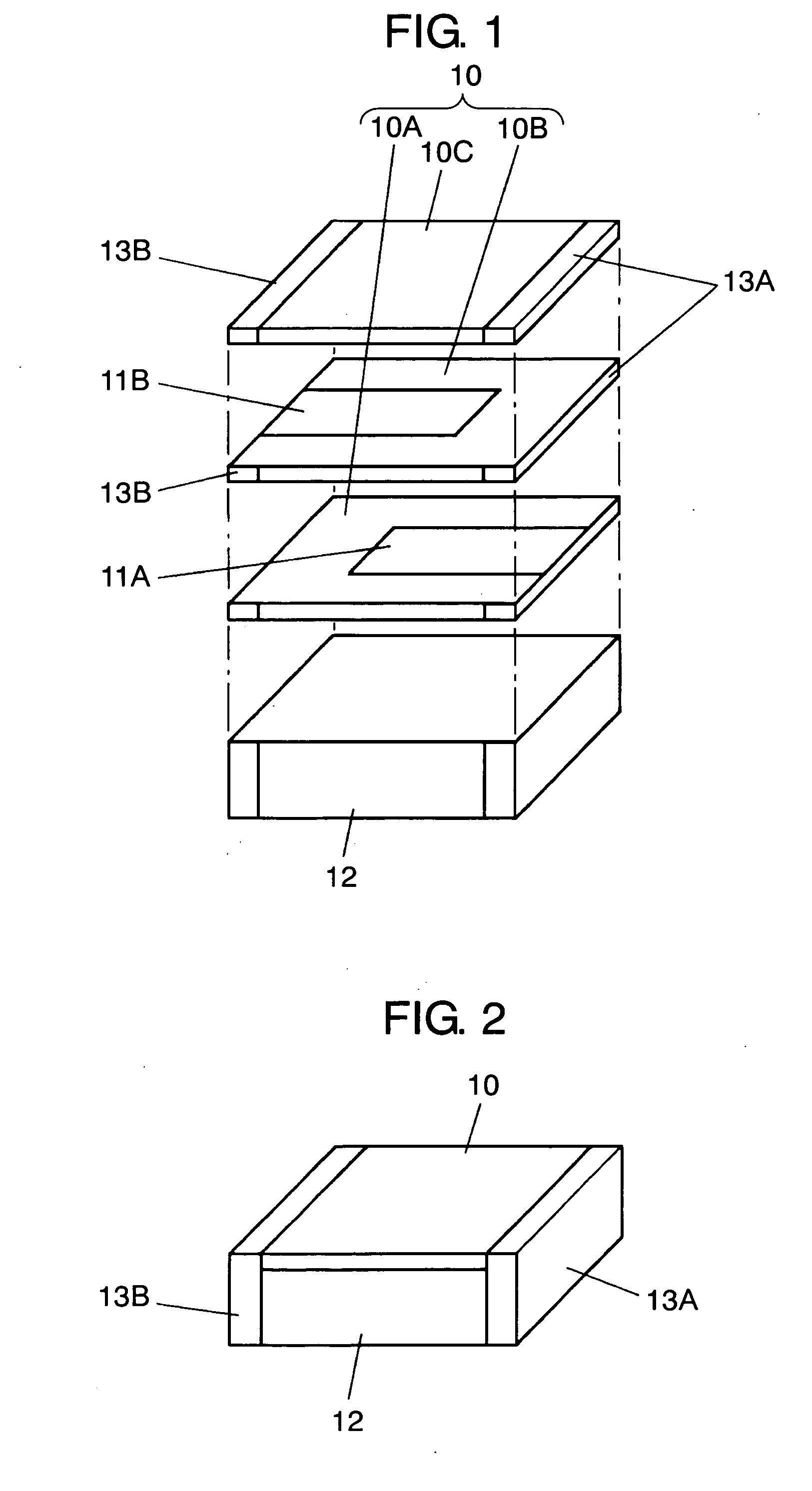
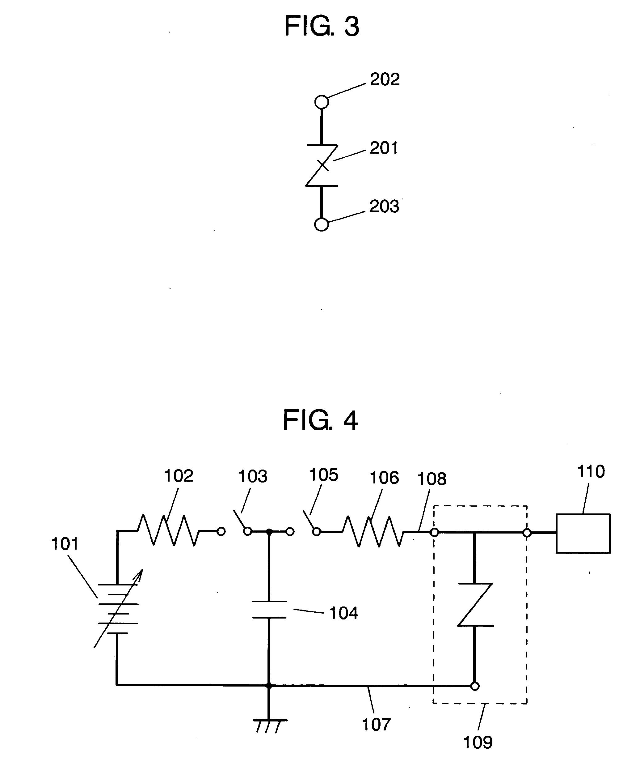
[0056]FIG. 1 is a schematic, exploded, perspective view showing an electrostatic discharge protection component according to a first embodiment of the invention. FIG. 2 is a perspective view showing an outward appearance of the electrostatic discharge protection component. FIG. 3 is an equivalent circuit diagram of the electrostatic discharge protection component.
[0057] As shown in FIGS. 1 and 2, the electrostatic discharge protection component according to the embodiment includes varistor layers 10A, 10B, 10C and internal electrodes 11A, 11B alternately laminated on ceramic insulating substrate 12, and a pair of external electrodes 13A, 13B provided on a ceramic sintered body formed by integrating the varistor layers and the internal electrodes. After varistor layer 10A is formed, internal electrode 11A is formed in a position as shown on varistor layer 10A. Thereafter, varistor layer 10B is laminated, internal electrode 11B is formed in a predetermined position on varistor layer ...
second embodiment
[0080]FIG. 5 is a schematic, exploded, perspective view showing an electrostatic discharge protection component according to a second embodiment of the invention. FIG. 6 is a perspective view showing an outward appearance of the electrostatic discharge protection component. In addition, an equivalent circuit diagram of the electrostatic discharge protection component according to the embodiment is the same as that shown in FIG. 3 and illustrated with respect to the electrostatic discharge protection component according to the first embodiment.
[0081] As shown in FIGS. 5 and 6, the electrostatic discharge protection component according to the embodiment includes varistor unit 50, external electrodes 14A, 14B, and protective film 18, which are formed on ceramic insulating substrate 12. Varistor layers 10D, 10E, internal electrode 11C, and external electrodes 14A, 14B are laminated to make varistor unit 50, and this varistor unit 50 is stuck to ceramic insulating substrate 12 to be sin...
third embodiment
[0102]FIG. 7 is a schematic, exploded, perspective view showing an electrostatic discharge protection component according to a third embodiment of the invention. FIG. 8 is a perspective view showing an outward appearance of the electrostatic discharge protection component. FIG. 9 is an equivalent circuit diagram of the electrostatic discharge protection component.
[0103] As shown in FIGS. 7 and 8, the electrostatic discharge protection component according to the embodiment includes varistor unit 70, glass / ceramic substrate 20 with an internal inductor, external electrode 15A for grounding, input external electrode 15B, and output external electrode 15C. According to the embodiment, the glass / ceramic substrate corresponds to a ceramic insulating substrate referred to in the invention. In the following descriptions, the glass / ceramic substrate is described as ceramic insulating substrate 20 or glass / ceramic substrate 20.
[0104] Varistor unit 70 includes varistor layers 10F, 10G, 10H a...
PUM
 Abstract
Description
Claims
Application Information


