Semiconductor memory device

a memory device and semiconductor technology, applied in semiconductor devices, digital storage, instruments, etc., can solve the problem of low flexibility in setting the voltage to be applied to the word line, and achieve the effect of increasing the number of wirings that form memory cell arrays and increasing the area of memory cell arrays

Inactive Publication Date: 2006-10-12
RENESAS ELECTRONICS CORP
View PDF7 Cites 38 Cited by
  • Summary
  • Abstract
  • Description
  • Claims
  • Application Information

AI Technical Summary

Benefits of technology

[0013] As described above, in the memory cell having the gain-cell structure shown in FIG. 29B, at least three levels of potential of the word line WL are required. Also, in consideration of the capacitance of the capacitor C and variations in threshold of the write transistor M2 and the read transistor M1, an operation margin of the transistors with respect to the voltage to be applied to the word line is small, and therefore there is a high possibility that malfunction will occur.
[0014] Furthermore, in the memory cell as shown in FIG. 29C, the word line for writing and the word line for

Problems solved by technology

Consequently, there is a problem of low flexibility

Method used


Image

  • Semiconductor memory device
  • Semiconductor memory device
  • Semiconductor memory device

Examples


first embodiment

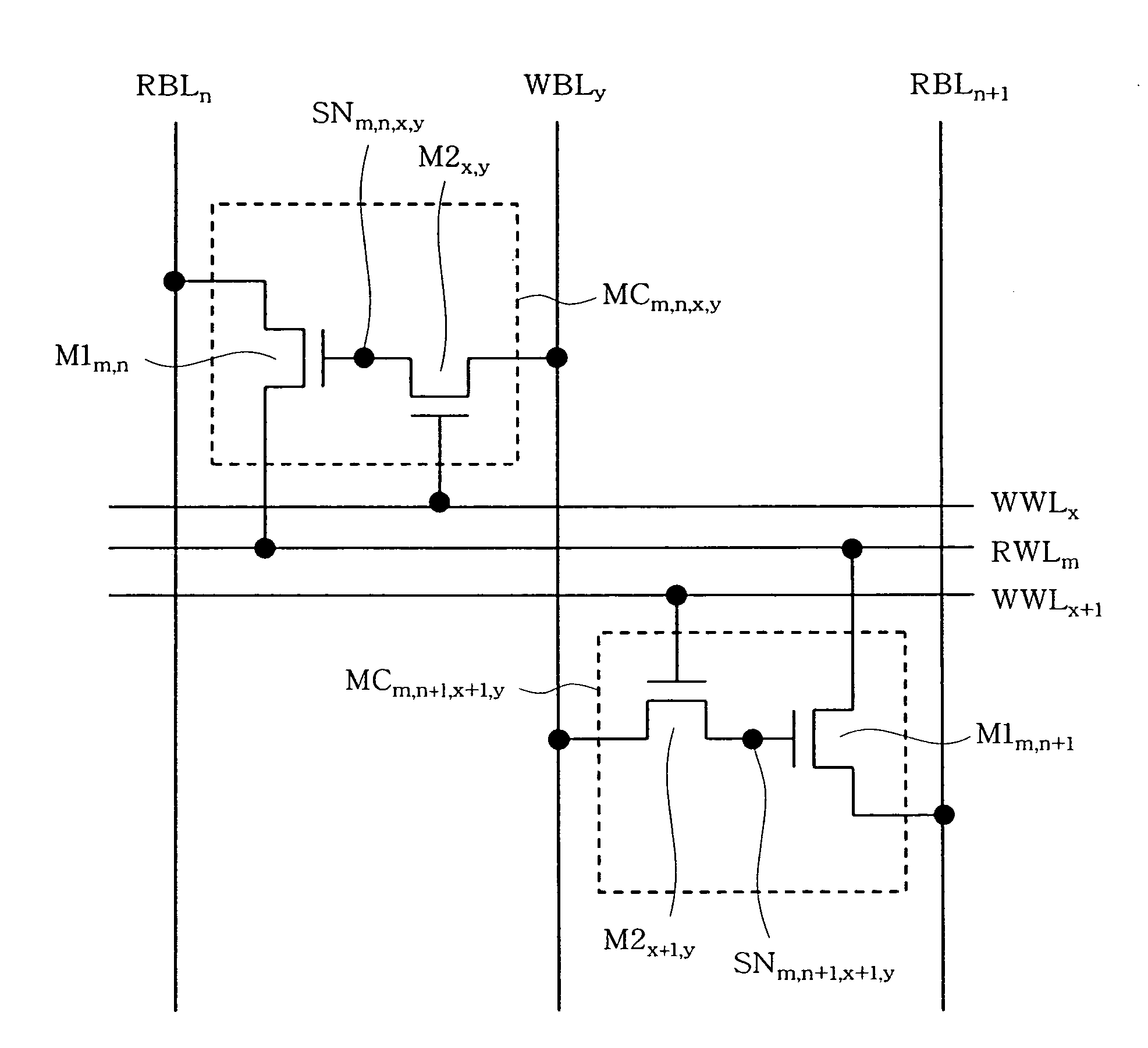
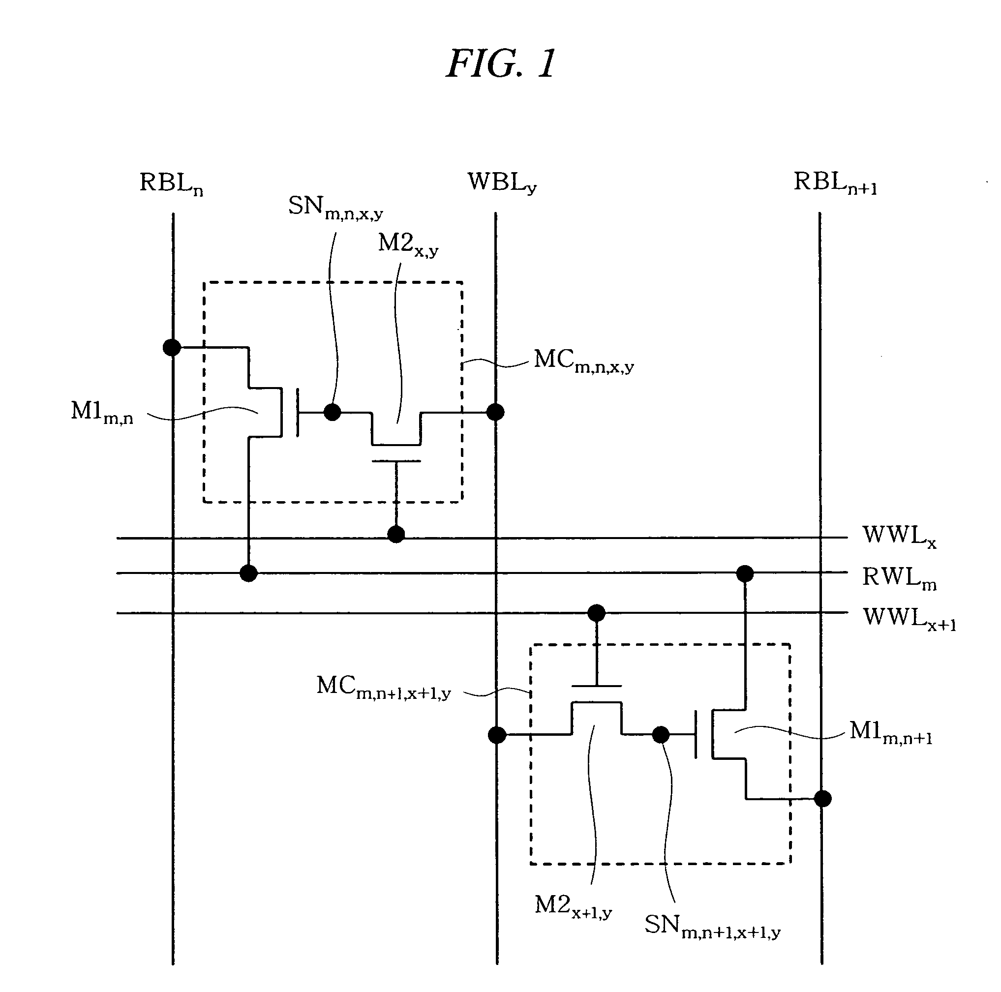
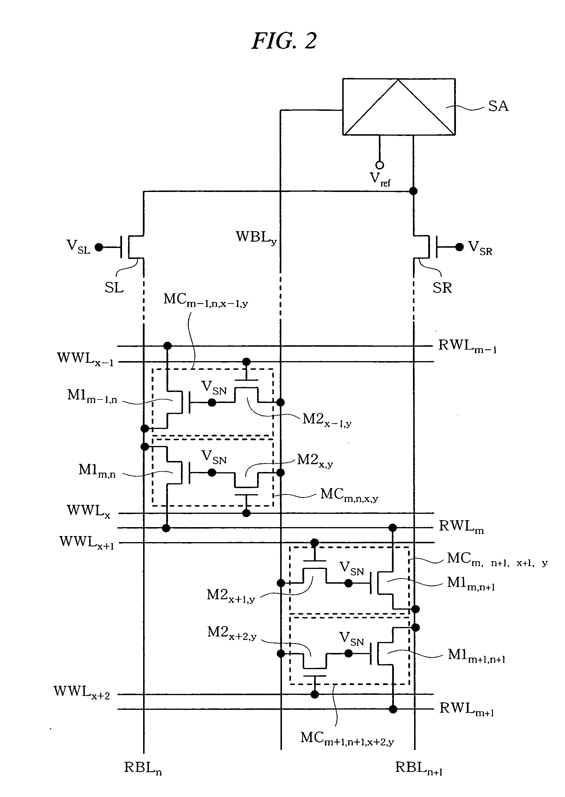
[0067]FIG. 1 is a drawing of an equivalent circuit, showing the structure and a connecting relation of a memory cell according to a first embodiment of the present invention. Note that it is assumed in the following description that wirings, memory cells, and transistors with the same suffixes (m, n, x, y: natural numbers) have a connecting relation. Also, although the case where the channel conduction type of a read transistor M1 and a write transistor M2 is n type will be described, both p type and n type can be used as the channel conduction type of the read transistor M1 and the write transistor M2. In this case, the magnitude of voltage and the direction of an electric current are changed.

[0068] First, one example of the structure of the memory cell according to the first embodiment will be described with reference to FIG. 1. A memory cell MCm,n,x,y according to the first embodiment includes a read transistor M1m,n and a write transistor M2x,y. The write transistor M2x,y has a...

second embodiment

[0096] In a memory cell MC according to a second embodiment, a write transistor M2, a read transistor M1, and a connecting relation among wirings are basically identical to those in the above-described first embodiment. However, Schottky connection is used for the contact between the drain of the read transistor M1 and read bit lines RBL. By doing so, it is possible to obtain an effect of preventing a current from flowing between read word lines RWL in the case where the potential relation is as represented by the equation (4) in the first embodiment.

[0097]FIG. 7 and FIG. 8 depict equivalent circuits each showing a connecting relation between the memory cells MC and wirings in the second embodiment. SD denotes a Schottky diode in Schottky connection.

[0098] Also, FIG. 9 depicts a read operation of the memory cell MC in the second embodiment. The principle of a read operation is basically identical to that in the first embodiment. However, in the case of the above-mentioned Schottky...

third embodiment

[0103] A third embodiment has a structure based on the second embodiment, in which an impurity diffused layer of an adjacent memory cell is used as a drain region of the read transistor M1 and the read transistor is connected to the read bit line RBL through a Schottky connection. Also, a thin-film transistor is used as the write transistor M2. Since the drain region is shared with the read transistor M1 of the adjacent memory cell, an effect of reducing the memory cell area can be achieved.

[0104]FIG. 12 is a drawing of an equivalent circuit showing a part of a memory cell array according to the third embodiment. The structure of a memory cell is identical to that in FIG. 7.

[0105]FIG. 13A to FIG. 13C and FIG. 14 depict the structure of memory cells forming the memory cell array and the memory cell array according to the third embodiment. FIG. 13A is a top view of the memory cell, FIG. 13B and FIG. 13C are cross-sectional views of the memory cell in FIG. 13A taken along an A-A′ sec...


PUM


Abstract

In a two-transistor gain cell structure, a semiconductor memory device capable of stable reading without malfunction and having small-area memory cells is provided. In a two-transistor gain cell memory having a write transistor and a read transistor, a write word line, a read word line, a write bit line, and a read bit line are separately provided, and voltages to be applied are independently set. Furthermore, a memory cell is connected to the same read word line and write bit line as those of an adjacent memory cell.

Description

CROSS-REFERENCE TO RELATED APPLICATION [0001] The present application claims priority from Japanese Patent Application No. JP 2005-112495 filed on Apr. 8, 2005, the content of which is hereby incorporated by reference into this application. TECHNICAL FIELD OF THE INVENTION [0002] The present invention relates to a semiconductor memory device. More particularly, it relates to a technology effectively applied to a memory having a two-transistor gain cell structure. BACKGROUND OF THE INVENTION [0003] For example, technologies regarding semiconductor memory devices studied by the inventors include the following technologies. [0004] In a one-transistor one-capacitor DRAM (Dynamic Random Access Memory) typical as a high-density large-capacity semiconductor memory, as shown in FIG. 29A, a transistor M which is turned ON / OFF by the potential of a word line WL and a memory capacitor C are connected in series between a bit line BL and a common potential line (for example, ground potential GND...

Claims


Application Information

Patent Timeline
IPC IPC(8): G11C8/00
CPCG11C7/18G11C11/405G11C2211/4013H01L27/0207H01L27/108G11C11/4097H10B12/00A01K93/00A01K91/04A01K95/00
Inventor KAMESHIRO, NORIFUMITAKEMURA, RIICHIROISHII, TOMOYUKI
Owner RENESAS ELECTRONICS CORP
Why Eureka
Try Eureka