Organic electroluminescent device

a technology of electroluminescent devices and organic el, which is applied in the direction of discharge tube luminescnet screens, natural mineral layered products, transportation and packaging, etc., can solve the problems of shortened half-life of the initial luminance of the organic el device, low efficiency, and formation of exciplexes or charge-transfer complexes with adjacent layers, etc., to achieve long initial luminance half-life and high luminous efficiency

Inactive Publication Date: 2006-10-12
TOYOTA IND CORP
View PDF4 Cites 107 Cited by
  • Summary
  • Abstract
  • Description
  • Claims
  • Application Information

AI Technical Summary

Benefits of technology

[0005] An object of the present invention is to provide an organic EL device that has a high luminous efficiency and a long half-life of the initial luminance.

Problems solved by technology

Although organic EL devices using a silole derivative or a phenanthroline derivative have a high efficiency, the problem is that an exciplex or a charge-transfer complex tends to be formed with adjacent layers due to the high electron mobility.
When at least one material of the organic compound-containing layers of an organic EL device forms an exciplex or a charge-transfer complex, these excitons have weak light emission, and this results in a low efficiency and a shortened half-life of the initial luminance of the organic EL device.

Method used


Image

  • Organic electroluminescent device
  • Organic electroluminescent device
  • Organic electroluminescent device

Examples


example 1

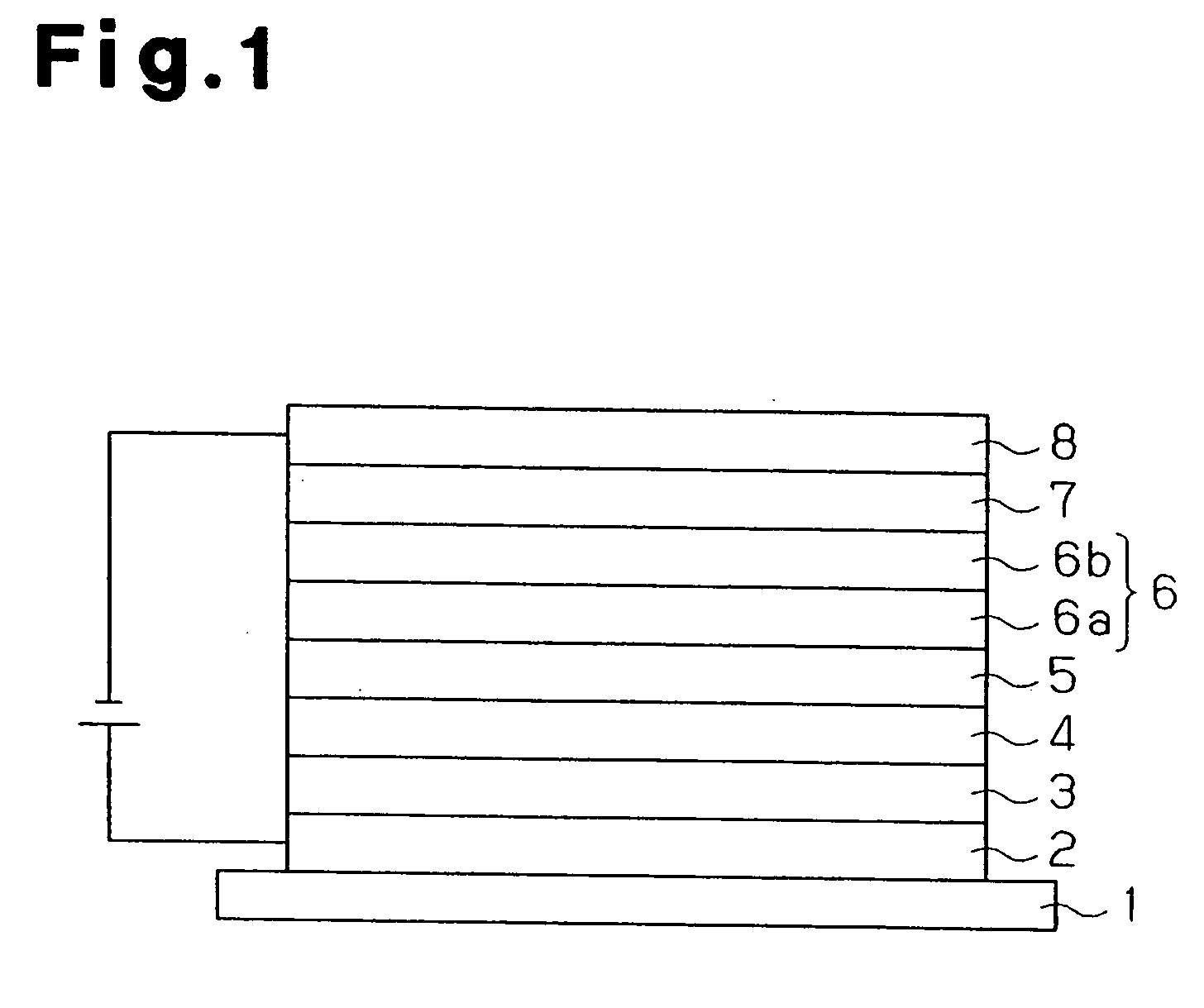
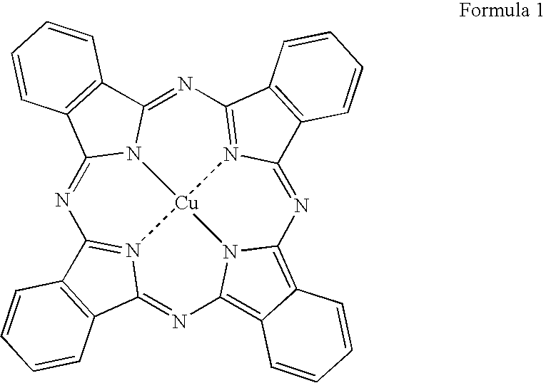
[0037] A transparent glass substrate was used as the substrate 1. An anode 2 was formed on the substrate 1. The anode 2 was formed of ITO having a thickness of 190 nm. For cleaning the substrate before vapor depositing an organic layer, the substrate 1 was subjected to alkali cleaning followed by washing with pure water, dried and then subjected to ultraviolet-ozone cleaning. The substrate 1 was then placed in a vacuum chamber, and CuPc shown in formula 1 was vapor deposited on the ITO provided on the substrate 1 with a carbon crucible at a deposition rate of 0.1 nm / s under a vacuum of about 5.0×10⁻⁵ Pa to form a hole injection region 3 of 10 nm in thickness.

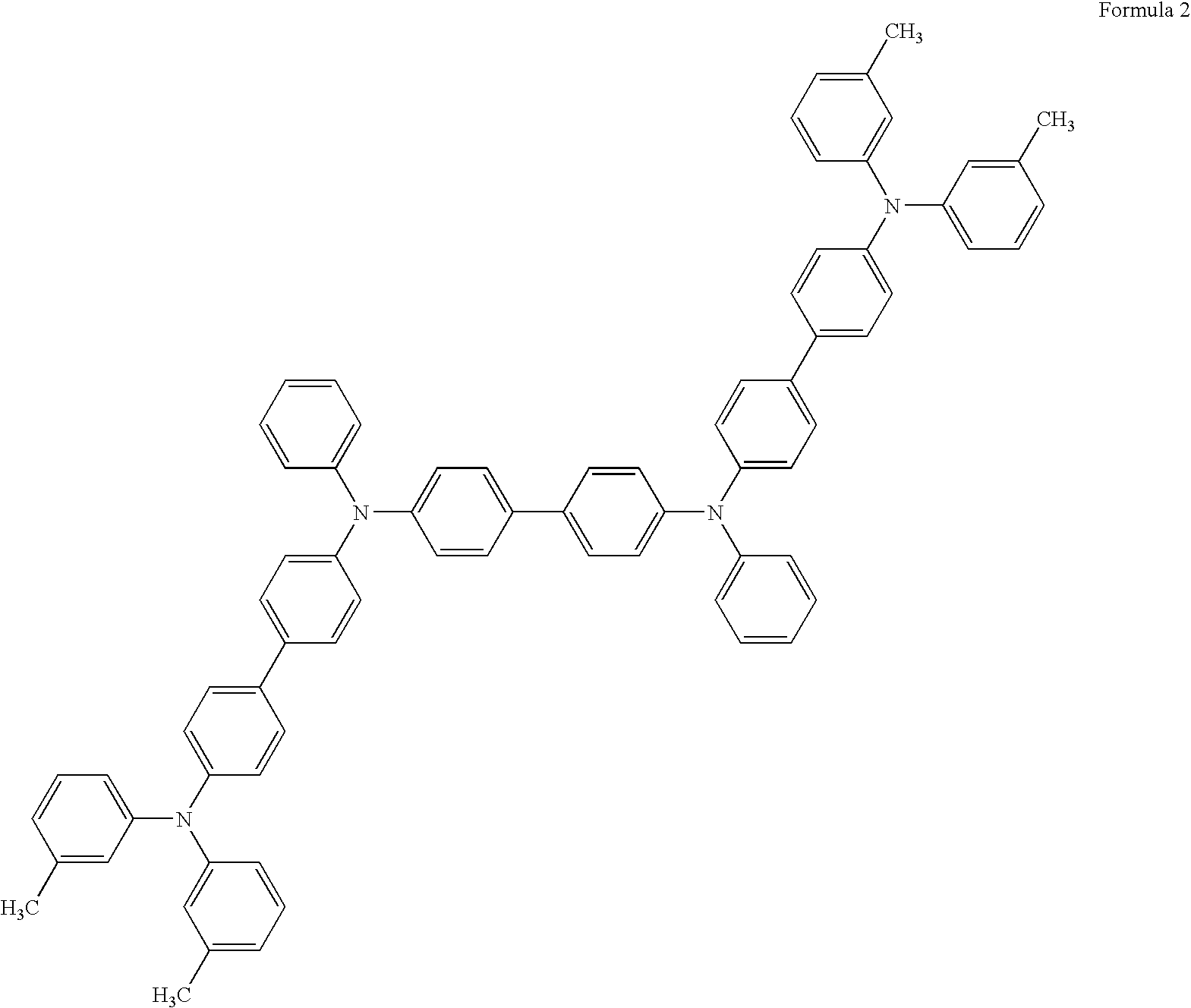
[0038] A triphenylamine tetramer shown in formula 2 was vapor deposited on the hole injection region 3 with a carbon crucible at a deposition rate of 0.1 nm / s under a vacuum of about 5.0×10⁻⁵ Pa to form a hole transport region 4 of 10 nm in thickness. The triphenylamine tetramer has electron mobility higher than that of CuPc w...

examples 2 to 7

[0049] In Examples 2 to 7, the thickness of the first electron transport layer 6a (Alq3) was each 3.0 nm (Example 2), 2.5 nm (Example 3), 2.0 nm (Example 4), 1.5 nm (Example 5), 1.0 nm (Example 6) and 0.5 nm (Example 7). Devices were prepared in the same manner as in Example 1 except for the above.

examples 8 to 14

[0054] In Examples 8 to 14, a device was produced under the same conditions as in Example 1 except that the second electron transport layer 6b was formed of bathocuproin represented by formula 6, which is a phenanthroline derivative. The thickness of the first electron transport layer 6a was 4.0 nm in Example 8, 3.0 nm in Example 9, 2.5 nm in Example 10, 2.0 nm in Example 11, 1.5 nm in Example 12, 1.0 in Example 13 and 0.5 nm in Example 14.


PUM

PropertyMeasurementUnit
thicknessaaaaaaaaaa
thicknessaaaaaaaaaa
thicknessaaaaaaaaaa

Abstract

The organic EL device of the present invention includes a plurality of organic compound-containing layers provided between a cathode and an anode. Of two of the organic compound-containing layers adjacent to each other, one layer positioned nearer the anode has electron mobility lower than that of the other layer positioned nearer the cathode. Accordingly, the organic EL device of the present invention has a high luminous efficiency and a long half-life of the initial luminance.

Description

TECHNICAL FIELD [0001] The present invention relates to an organic electroluminescent device (organic EL device). BACKGROUND ART [0002] Organic EL devices have been attracting attention as next-generation display devices. Generally, organic EL devices are fabricated by forming an anode composed of a transparent conductive material such as indium tin oxide (ITO) on a glass substrate and laminating, on the anode, a hole injection region, a hole transport region, a light emission region, an electron transport region and a cathode in that order. Organic EL devices with such configuration emit light upon application of a direct-current voltage between the anode and the cathode. Specifically, when a direct-current voltage is applied between the anode and the cathode, holes are injected from the anode and electrons are injected from the cathode. Holes move to the light emission region through the hole injection region and the hole transport region, while electrons move to the light emissio...

Claims


Application Information

Patent Timeline
Patent Type & Authority Applications(United States)
IPC IPC(8): H01L51/54H05B33/12C09K11/06H01L51/00H01L51/50H05B33/14H05B33/22
CPCC09K11/06Y10T428/24942C09K2211/1014C09K2211/1029C09K2211/1074C09K2211/1096C09K2211/188H01L51/005H01L51/0059H01L51/0071H01L51/0078H01L51/0081H01L51/0094H01L51/50H01L51/5048H01L51/5092H05B33/14C09K2211/1007H10K85/60H10K85/631H10K85/657H10K85/311H10K85/324H10K85/40H10K50/00H10K50/14H10K50/171H05B33/22
Inventor NAGARA, YOSHIAKI
Owner TOYOTA IND CORP
Why Eureka
Try Eureka